Optical proximity correction method

a technology of optical proximity and correction method, applied in the field of optical proximity correction method, can solve the problems of angled corner rounding, line end shortening, line width increasing/decreasing, etc., and achieve the effect of simple operation, and reducing the difference in pattern density

Inactive Publication Date: 2005-01-13
UNITED MICROELECTRONICS CORP
View PDF2 Cites 153 Cited by
  • Summary
  • Abstract
  • Description
  • Claims
  • Application Information

AI Technical Summary

Benefits of technology

[0010] According to the claimed invention, an optical proximity correction (OPC) method is provided. The method first provides a predetermined integrated circuit layout. The integrated circuit layout is then formed on a surface of a photo-mask, and a plurality of transparent nonprintable dummy patterns are formed outside the integrated circuit layout on the surface of the photo-mask. The plurality of transparent dummy patterns are used to reduce the difference in pattern density on the surface of the photo-mask so as to modify optical proximity effect, and the dummy patterns are not transferred to a photoresist layer formed on a semiconductor wafer during a photolithography process because of a phase difference of 0 or 180 degrees between a transmitted light of the integrated circuit layout and a transmitted light of the dummy patterns.
[0011] It is an advantage over the prior art that the OPC method of the claimed invention forms a plurality of nonprintable dummy patterns around an integrated circuit layout predetermined to be transferred on a substrate. The dummy patterns are used to reduce the difference in pattern density of the integrated circuit layout for correcting optical proximity effect. Furthermore, the dummy patterns are designed by performing a simple operation according to conditions of a photolithographic process. Therefore, the time cost of a complicated operation performed by the prior art OPC method can be substantially reduced.

Problems solved by technology

The optical proximity effect will cause defects when transferring the photo-mask pattern, such as right-angled corner rounding, line end shortening, and line width increasing / decreasing.
However, the subresolution grating is not able to suppress the optical proximity effect when transferring the photo-mask pattern.
The prior art OPC method only uses one OPC model to correct the whole integrated circuit layout, and the factor of different pattern density in local regions of the photo-mask resulting in overexposure or underexposure is not taken into consideration.
Therefore, the pattern density of integrated circuit layout is very different in local regions of the chip, and the prior art OPC method is not applicable.

Method used


Image

  • Optical proximity correction method
  • Optical proximity correction method
  • Optical proximity correction method

Examples


Embodiment Construction

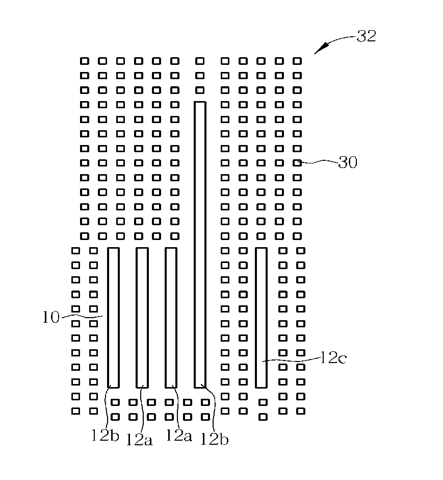
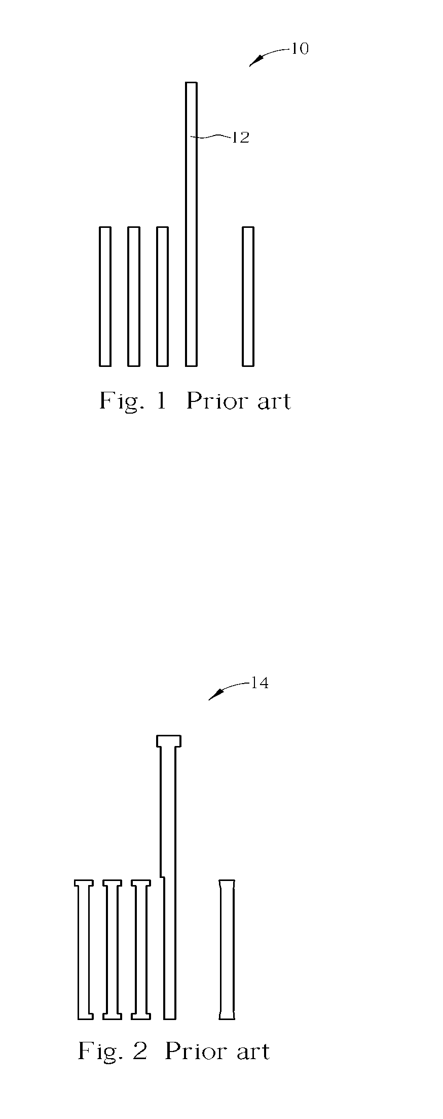
[0015] Please refer to FIG. 5 and FIG. 6. FIG. 5 and FIG. 6 respectively depict the integrated circuit layouts 10, 16 of FIG. 1 and FIG. 3 after correcting by an OPC method according to the present invention method. As shown in FIG. 5, according to the present invention method, the integrated circuit layout 10 predetermined to be transferred to a substrate (not shown), such as a semiconductor wafer, is directly formed on a surface of a photo-mask (not shown). The integrated circuit layout 10 includes a plurality of figures, such as dense line FIG. 12a, semi-dense line FIG. 12b and at least an isolated line FIG. 12c. However, the integrated circuit layout 10 is not limited to include line figures only. The integrated circuit layout 10 can include figures in various shapes and in different pattern density according to the present invention.

[0016] Moreover, a plurality of dummy patterns 30 of rectangular figures are formed in a blank region outside the integrated circuit layout 10 on ...


PUM

PropertyMeasurementUnit
optical proximity correctionaaaaaaaaaa
optical proximityaaaaaaaaaa
densityaaaaaaaaaa

Abstract

An integrated circuit layout includes dense figures and at least one isolated figure. A plurality of dummy patterns are formed to surround the isolated figure, so as to reduce the difference in pattern density of the integrated circuit layout. A transmitted light of the dummy patterns provides a phase difference of 0 or 180 degrees relative to a transmitted light of the integrated circuit layout. The integrated circuit layout and the plurality of dummy patterns are formed on a photo-mask.

Description

CROSS REFERENCE TO RELATED APPLICATIONS [0001] This is a continuation-in-part of U.S. application Ser. No. 10 / 064,413, filed on Jul. 11, 2002, and which is included herein by reference.BACKGROUND OF INVENTION [0002] 1. Field of the Invention [0003] The present invention relates to an optical proximity correction (OPC) method, and more particularly, to an OPC method using dummy patterns to reduce the difference in pattern density. [0004] 2. Description of the Prior Art [0005] In semiconductor manufacturing processes, in order to transfer an integrated circuit layout onto a semiconductor wafer, the integrated circuit layout is first designed and formed as a photo-mask pattern. The photo-mask pattern is then proportionally transferred to a photoresist layer positioned on the semiconductor wafer. [0006] As the design pattern of integrated circuit becomes smaller and due to the resolution limit of the optical exposure tool, optical proximity effect will easily occur during the photolitho...

Claims


Application Information

Patent Timeline
Patent Type & Authority Applications(United States)
IPC IPC(8): G03F1/00G03F1/14
CPCG03F1/144G03F1/36G03F1/26
Inventor HWANG, JIUNN-RENHUANG, JUI-TSENHSIEH, CHANG-JYH
Owner UNITED MICROELECTRONICS CORP
Why Eureka
Try Eureka