
System and method for validating and visualizing APC assisted semiconductor manufacturing processes

a technology of advanced process control and manufacturing process, applied in adaptive control, instruments, computing, etc., can solve the problems of difficult variable processing constraints, and general processing constraints, and achieve tighter control over the manufacturing process. , to achieve the effect of maximizing the benefits of the manufacturing process, it is difficult to control the manufacturing process

Inactive Publication Date: 2005-01-13
BLUE CONTROL TECH
View PDF7 Cites 52 Cited by
  • Summary
  • Abstract
  • Description
  • Claims
  • Application Information

AI Technical Summary

Benefits of technology

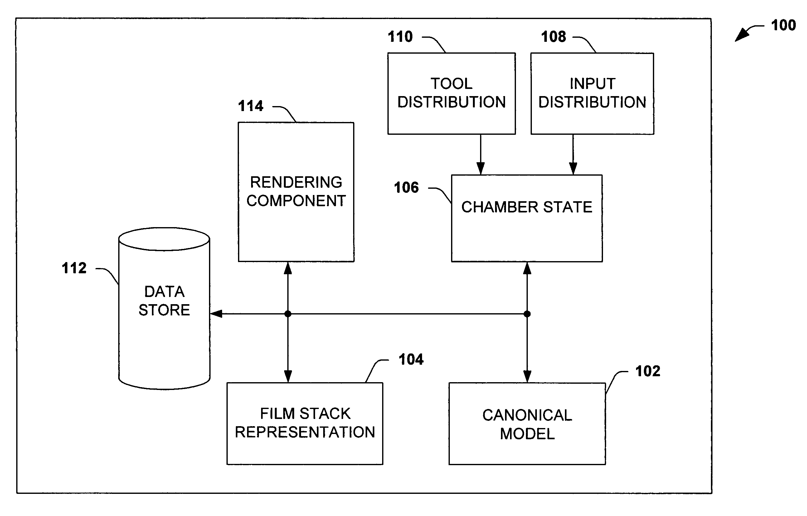
"The invention is a system and method for simulating a semiconductor manufacturing process using an APC assisted system. The system uses a canonical model to predict the process rates based on the materials and parameters of the process. The system also includes a film stack representation to show the layers and blocks of materials exposed during the process. The system captures the process chamber state at pre-defined time intervals and relays it to the canonical model. The system can also update the film stack representation based on the predicted process rates and control values. The invention provides a customizable tool for validating the semiconductor manufacturing process and ensuring it meets output specifications. The system can also help identify and troubleshoot issues with the process."

Problems solved by technology

However, tighter control over the manufacturing process can be difficult to achieve, especially as critical dimensions decrease further.
Typically, in heat treatment operations, no additional material is added or removed from the wafer, although contaminates and vapors may evaporate from the wafer.
Additionally, these variables are generally subject to processing constraints that facilitate reduction or prevention of damage to the wafer and / or semiconductor device.
Due to number of variables involved, constraints on those variables, and desire to create favorable device characteristics while suppressing undesirable device characteristics, it can be difficult to control a manufacturing process let alone maximize benefits of the manufacturing process.
It has been empirically observed that controlling the manufacturing process becomes even more challenging as smaller and smaller devices need to be fabricated.
However, more complex predictive models that utilize a higher number of variables are more difficult to solve, and are often nonlinear, thus further increasing difficulty in solving the predictive models.
Moreover, validation of a generated complex process model can become expensive and inefficient, as conventional systems and / or methods of validating predictive models require empirical results from a test wafer and / or processed wafers.
Such conventional validation of a predictive model is expensive and inefficient, as the testing consumes test wafers and / or actual wafers, tool time, operator time, etc.
Moreover, after incurring testing expenses the predictive model can remain faulty, as expenses increase with a number of process variables modified.

Method used


Image

  • System and method for validating and visualizing APC assisted semiconductor manufacturing processes
  • System and method for validating and visualizing APC assisted semiconductor manufacturing processes
  • System and method for validating and visualizing APC assisted semiconductor manufacturing processes

Examples


Embodiment Construction

The present invention is now described with reference to the drawings, wherein like reference numerals are used to refer to like elements throughout. In the following description, for purposes of explanation, numerous specific details are set forth in order to provide a thorough understanding of the present invention. It may be evident, however, that the present invention may be practiced without these specific details. In other instances, well-known structures and devices are shown in block diagram form in order to facilitate describing the present invention.

As used in this application, the term “computer component” is intended to refer to a computer-related entity, either hardware, a combination of hardware and software, software, or software in execution. For example, a computer component may be, but is not limited to being, a process running on a processor, a processor, an object, an executable, a thread of execution, a program, and / or a computer. By way of illustration, both...


PUM


Abstract

A system and / or methodology that facilitates verifying and / or validating an APC assisted process via simulation is provided. The system comprises a film stack representation and a canonical model. The canonical model can predict process rates based at least in part upon an exposed material in the film stack representation. A solver component can also be provided to generate an updated recipe set-point according inputs and outputs of the canonical model.

Description

TECHNICAL FIELD The present invention relates generally to semiconductor fabrication, and more particularly to validating and / or visualizing Advanced Process Control (APC) assisted semiconductor manufacturing processes. BACKGROUND OF THE INVENTION As dimensions of semiconductor devices decrease, available process window size decreases and manufacturing design rules shrink requiring tighter control over a manufacturing process. Generally, improvements in semiconductor fabrication processes and / or improvements in structural fabrication are required in order to further decrease critical dimensions and, thereby semiconductor devices. However, tighter control over the manufacturing process can be difficult to achieve, especially as critical dimensions decrease further. Semiconductor fabrication is a manufacturing process employed to create semiconductor devices in and on a wafer surface. Polished, blank wafers come into semiconductor fabrication, and exit with the surface covered with...

Claims


Application Information

Patent Timeline
Patent Type & Authority Applications(United States)
IPC IPC(8): G05B13/04H01L21/00
CPCH01L21/67276G05B13/048
Inventor PATEL, SUKESHRAHEJA, RAJ
Owner BLUE CONTROL TECH
Learn More