Organic electroluminescent device adapted for assembly function

a technology of electroluminescent devices and assemblies, applied in the direction of instruments, discharge tubes, luminescnet screens, etc., can solve the problems of wasting space and seriously harming the quality requirement of high resolution of oled devices, so as to reduce the area of the substrate exposed, reduce the size of the gap, and reduce the spacing

Inactive Publication Date: 2005-01-20
PENG KUAN CHANG
View PDF3 Cites 14 Cited by
  • Summary
  • Abstract
  • Description
  • Claims
  • Application Information

AI Technical Summary

Benefits of technology

[0007] Accordingly, it is a primary object of the present invention to provide an organic electroluminescent device adapted for assembly function, capable of covering the first electrodes and the second electrodes inside the isolating seal cap completely, resulting in greatly reducing the area of the substrate exposed outside the isolating seal cap, whereby the size of the gap may be reduced when assembling every two of the OLED devices, correspondingly reducing the size of the spacing between every two of the first electrodes or every two of the second electrodes as well. Therefore, the quality requirement for high resolution may be raised significantly.
[0008] It is a secondary object of the present invention to provide an organic electroluminescent device adapted for assembly function, capable of greatly reducing the area of the substrate, the first electrodes or the second electrodes exposed outside the isolating seal cap to a size being beneficial for assembling.
[0009] It is another object of the present invention to provide an organic electroluminescent device adapted for assembly function being beneficial for the flexible design in product specifications, by greatly reducing the area of the substrate, the first electrodes or the second electrodes exposed outside the isolating seal cap.

Problems solved by technology

For the purpose of having an identical pitch a4 between two adjacently-situated scanning lines or data lines (the distance between two adjacently-situated first electrodes or two adjacently-situated second electrodes) in the assembled OLED display device while viewing, the width of the a4 must be designed as equivalent to that of a gap a3, resulting in wasting the space when assembling the OLED device, further being seriously harmful to the quality requirement for high resolution of the OLED device.

Method used


Image

  • Organic electroluminescent device adapted for assembly function
  • Organic electroluminescent device adapted for assembly function
  • Organic electroluminescent device adapted for assembly function

Examples


Embodiment Construction

[0020] The structural features and the effects to be achieved may further be understood and appreciated by reference to the presently preferred embodiments together with the detailed description.

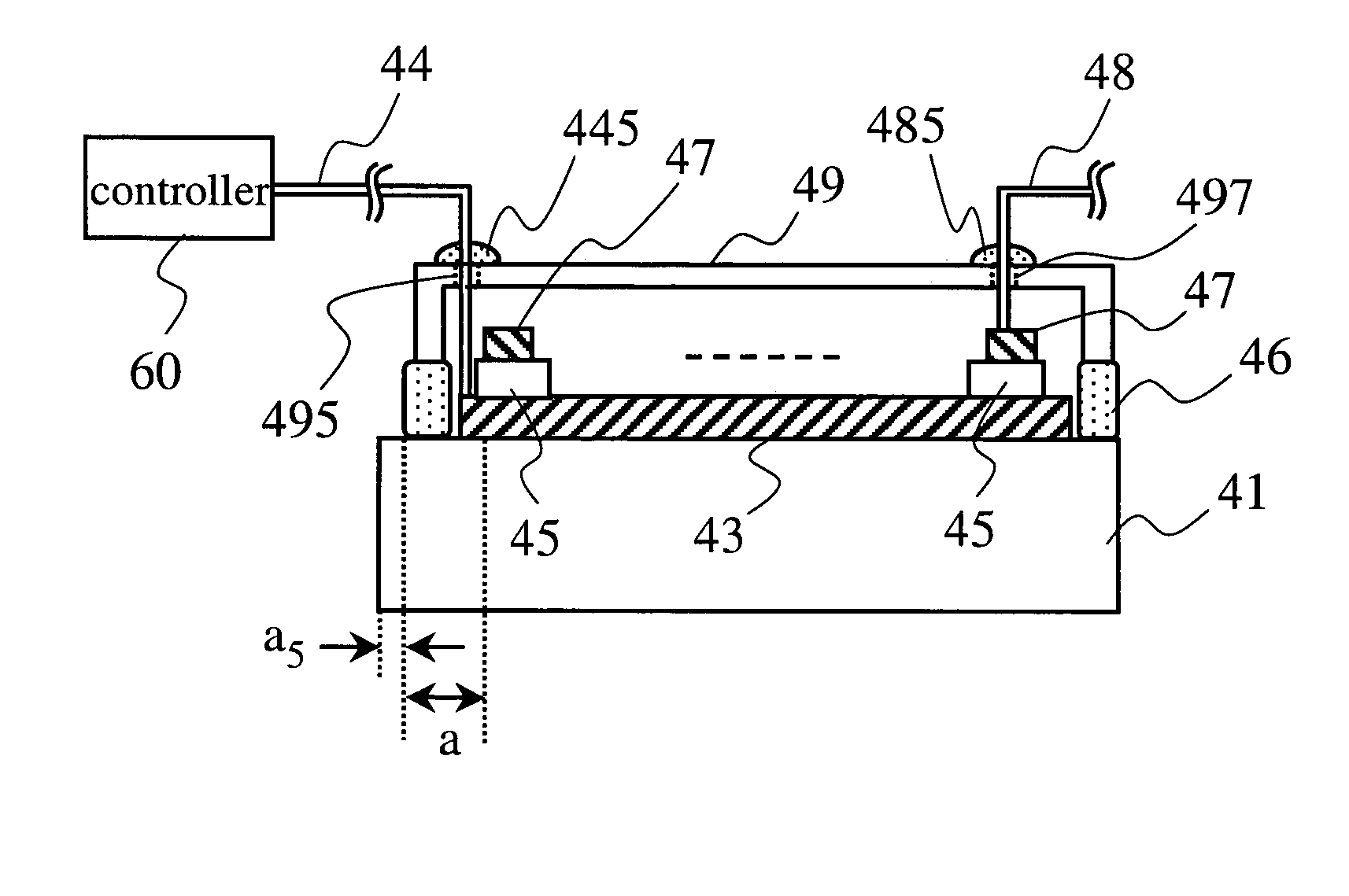
[0021] Firstly, referring to FIGS. 4 and 5, there are shown a structural cross-sectional view and a top view of an organic electroluminescent device of a preferred embodiment of the present invention; as illustrated in the figures, the present invention essentially comprises forming a first electrode 43 on a part of surface of a substrate 41, and forming at least one light-emitting layer45 including an organic emitting layer, and a second electrode 47 in turn, by vapor deposition, sputtering, chemical vapor thin-film deposition, or spray pyrolysis methods and so on, onto the appropriate position of the first electrode 43. Subsequently, an isolating seal cap 49 (or an isolating protecting layer) capable of covering and protecting the organic layer 45 may be erected, by a seal pad 46, on the ...


PUM

PropertyMeasurementUnit
widthaaaaaaaaaa
widthaaaaaaaaaa
widthaaaaaaaaaa

Abstract

An organic electroluminescent device adapted for assembly function of a greater display size is provided. The device comprises forming first electrodes, a light-emitting layer, second electrodes, and isolating seal cap in turn. One side of the isolating cap is chiseled to form at least one channel, each channel being passed through by a corresponding connecting line. The end faces of the connecting lines may be contacted with a part of surface the first electrodes or second electrodes formed inside the isolating seal cap. The side ends of the first electrodes and second electrodes may be not necessarily exposed outside the isolating seal cap, due to the fact that the contacting point between the first electrodes or second electrodes and the connecting lines may be formed inside the isolating seal cap, whereby the area of the substrate, the first electrodes, and the second electrodes exposed outside the isolating seal cap may be reduced, further greatly decreasing the size of the gap during the assembly for two light-emitting devices correspondingly as well. Not only adapting for the assembly for a larger-sized display device, but also effectively increasing the quality requirement for higher resolution of the light-emitting device may be provided.

Description

FIELD OF THE INVENTION [0001] The present invention is related to an organic electroluminescent device, particularly to an organic electroluminescent device adapted for assembly function. Not only adapting for the assembly for a larger-sized display device, but also effectively raising the quality requirement for high resolution of the electroluminescent device may be provided. BACKGROUND [0002] The organic electroluminescent device (referred to as an OLED device hereinafter) is focused and used by all circles, among new-generation display panels, owing to advantages of a large view angle, short response time, thin display thickness, lower power consumption, simple manufacturing process, endurance for collision, absence of backlight source, capability for emitting full-color light thereof. [0003] Referring to FIGS. 1 and 2, there are shown a structural cross-section view and a top view of a conventional OLED device, respectively. The conventional OLED device essentially comprises fo...

Claims


Application Information

Patent Timeline
Patent Type & Authority Applications(United States)
IPC IPC(8): G02F1/1335H01J1/62H01L27/15H01L27/32H01L35/24H01L51/10H01L51/52
CPCH01L27/3288H01L51/5237H01L27/3293H10K59/179H10K59/18H10K50/846H10K50/841
Inventor PENG, KUAN-CHANG
Owner PENG KUAN CHANG
Why Eureka
Try Eureka