
Lithographic apparatus and device manufacturing method

a technology of lithographic projection and manufacturing method, which is applied in the direction of electrical devices, printers, instruments, etc., can solve the problems of increasing the potential for contamination of the microlens array, the small working distance, and the increased potential for collision between the substrate and the microlens array, so as to minimize the absorption of inactive parts, reduce the working distance, and reduce the effect of inactivity

Inactive Publication Date: 2005-01-20
ASML NETHERLANDS BV
View PDF15 Cites 17 Cited by
  • Summary
  • Abstract
  • Description
  • Claims
  • Application Information

AI Technical Summary

Benefits of technology

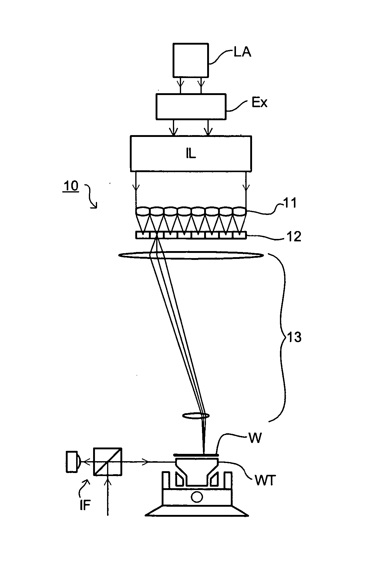
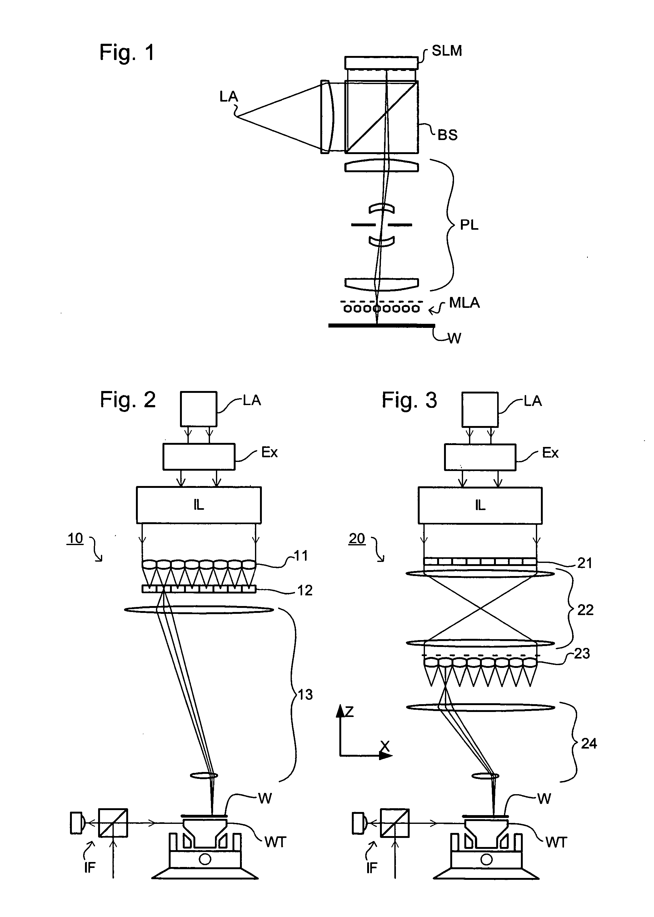
[0012] In one example, the illumination system delivers a substantially collimated beam of radiation to the microlens array, which forms the array of source images therefrom. The programmable patterning device is a selectively transmissive device (e.g., an LCD array) positioned proximate to the microlens array, whereby addressable elements of the programmable patterning device can be set to block respective ones of the source images. This provides a simple, robust system. To minimize absorption by inactive parts of the programmable patterning device, the programmable patterning device is placed close to the plane of the source images, so that each of the beams fits within the transmissive part of each addressable element of the programmable patterning device.
[0013] In another example, the projection system further comprises a second projection subsystem for projecting an image of the programmable patterning device onto the microlens array. The second projection subsystem can be a (refractive) lens system of known type and provides additional flexibility of design of the apparatus. For example, by designing the second projection subsystem with appropriate magnification or reduction, it becomes possible to use a programmable patterning device and a microlens arrays of different scales.
[0014] In one example, the microlens array can be arranged to project the source images onto a spherical surface. This allows the size of the elements making up the projection subsystem to be reduced.

Problems solved by technology

A small working distance is a drawback, and causes problems, such as increased potential for contamination of the microlens array and increased potential for collisions between substrate and the microlens array.
Also, little space is available for sensors, such as height and tilt sensors, which are used for leveling control during scanning exposures.

Method used


Image

  • Lithographic apparatus and device manufacturing method
  • Lithographic apparatus and device manufacturing method

Examples


Embodiment Construction

[0022] Overview and Terminology

[0023] While specific configurations and arrangements are discussed, it should be understood that this is done for illustrative purposes only. A person skilled in the pertinent art will recognize that other configurations and arrangements can be used without departing from the spirit and scope of the present invention. It will be apparent to a person skilled in the pertinent art that this invention can also be employed in a variety of other applications.

[0024] More information with regard to lithographic devices as here described can be found, for example, in U.S. Pat. No. 6,046,792, which is incorporated herein by reference in its entirety.

[0025] Additional information regarding manufacturing processes can be obtained, for example, from the book “Microchip Fabrication: A Practical Guide to Semiconductor Processing”, Third Edition, by Peter van Zant, McGraw Hill Publishing Co., 1997, ISBN 0-07-067250-4, which is incorporated herein by reference in i...


PUM


Abstract

A lithographic projection apparatus comprises a microlens array for generating a plurality of source images in a two-dimensional array, a programmable patterning means having a plurality of addressable elements acting as shutters for the source images and a projection subsystem for projecting a n image of the array of source images onto a substrate. A greater working distance can thereby be obtained

Description

BACKGROUND OF THE INVENTION [0001] 1. Field of the Invention [0002] The present invention relates to a lithographic projection apparatus and device manufacturing method. [0003] 2. Related Art [0004] Lithographic projection apparatus can be used, for example, in the manufacture of devices on substrates. For example, a lithographic projection apparatus can be used for the manufacture of integrated circuits (ICs). In such a case, the programmable patterning means can generate a circuit pattern corresponding to an individual layer of the IC, and this pattern can be imaged onto a target portion (e.g., comprising one or more dies) on a substrate (e.g., a silicon wafer) that has been coated with a layer of radiation-sensitive material (e.g., resist). [0005] In general, a single wafer will contain a whole network of adjacent target portions that are successively irradiated via the projection system, one at a time. In apparatus employing patterning by a mask on a mask table, a distinction ca...

Claims


Application Information

Patent Timeline
IPC IPC(8): G02B3/00G03F7/20H01L21/027
CPCG03F7/70291G03F7/70275G03F7/2057
Inventor VAN DER MAST, KAREL DIEDERICKBLEEKER, ARNO JANGUI, CHENG-QUNHOEFNAGELS, JOHAN CHRISTIAAN GERARD
Owner ASML NETHERLANDS BV
Learn More