Optical component and manufacture method of the same

Inactive Publication Date: 2005-01-20
PANASONIC CORP
View PDF2 Cites 66 Cited by
  • Summary
  • Abstract
  • Description
  • Claims
  • Application Information

AI Technical Summary

Benefits of technology

[0007] An optical component of the present invention comprises a concave package provided by layering ceramic substrates; a groove section formed at a bottom face in this package; a light-receiving element or a light-emitting element provided in this groove section; a cover provided to cover an opening section of the package; and a lens formed at this cover. Forming the lens at the cover enables an inexpensive optical component and the package by laye

Problems solved by technology

As a result, providing the through hole caused cost increase, and filling of low melting point glass 5 into the hole caused further cost increase for manufactur

Method used


Image

  • Optical component and manufacture method of the same
  • Optical component and manufacture method of the same
  • Optical component and manufacture method of the same

Examples


embodiment 1

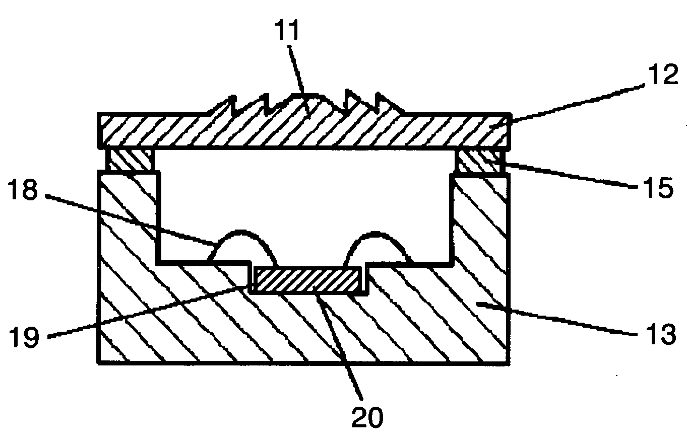
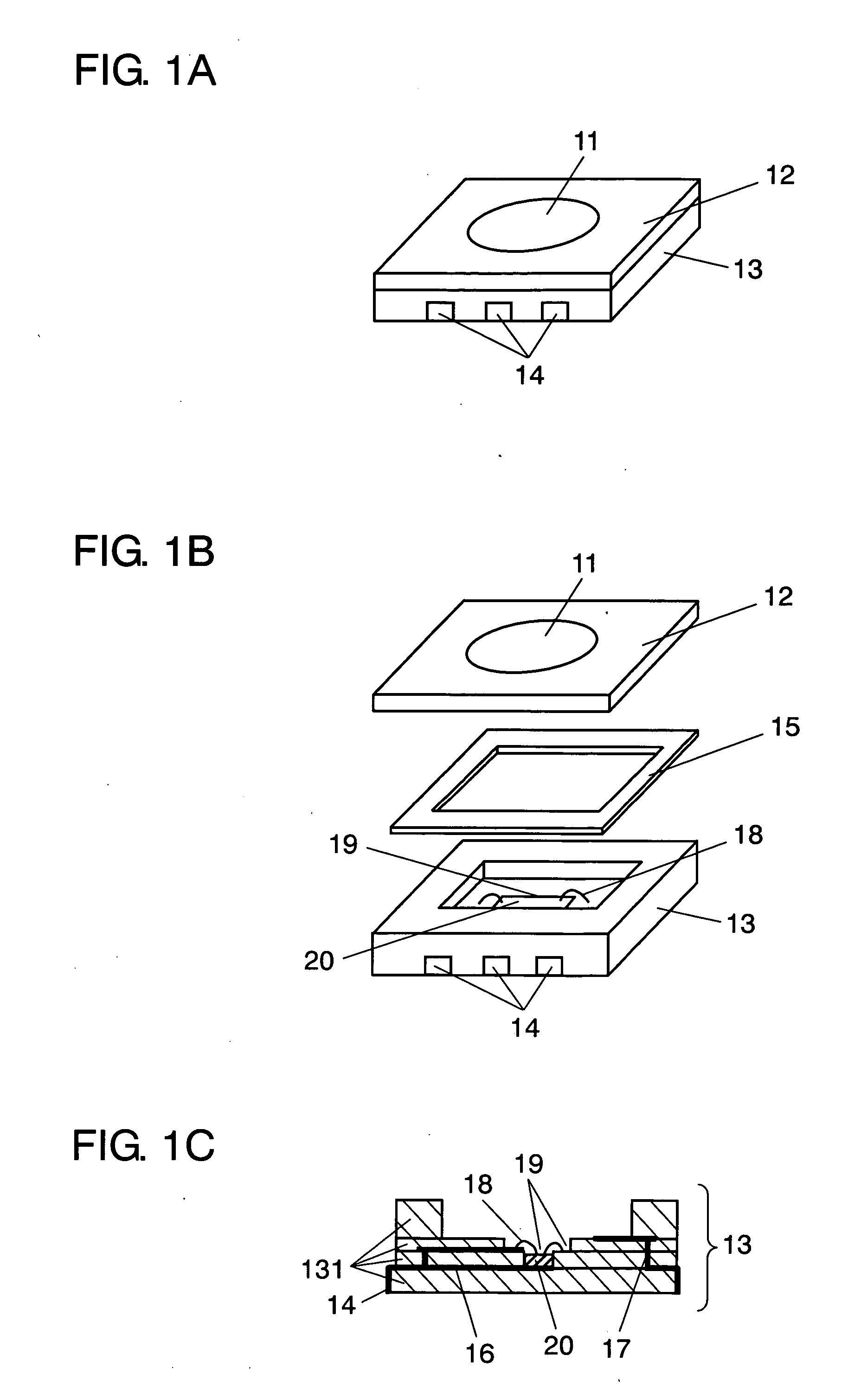
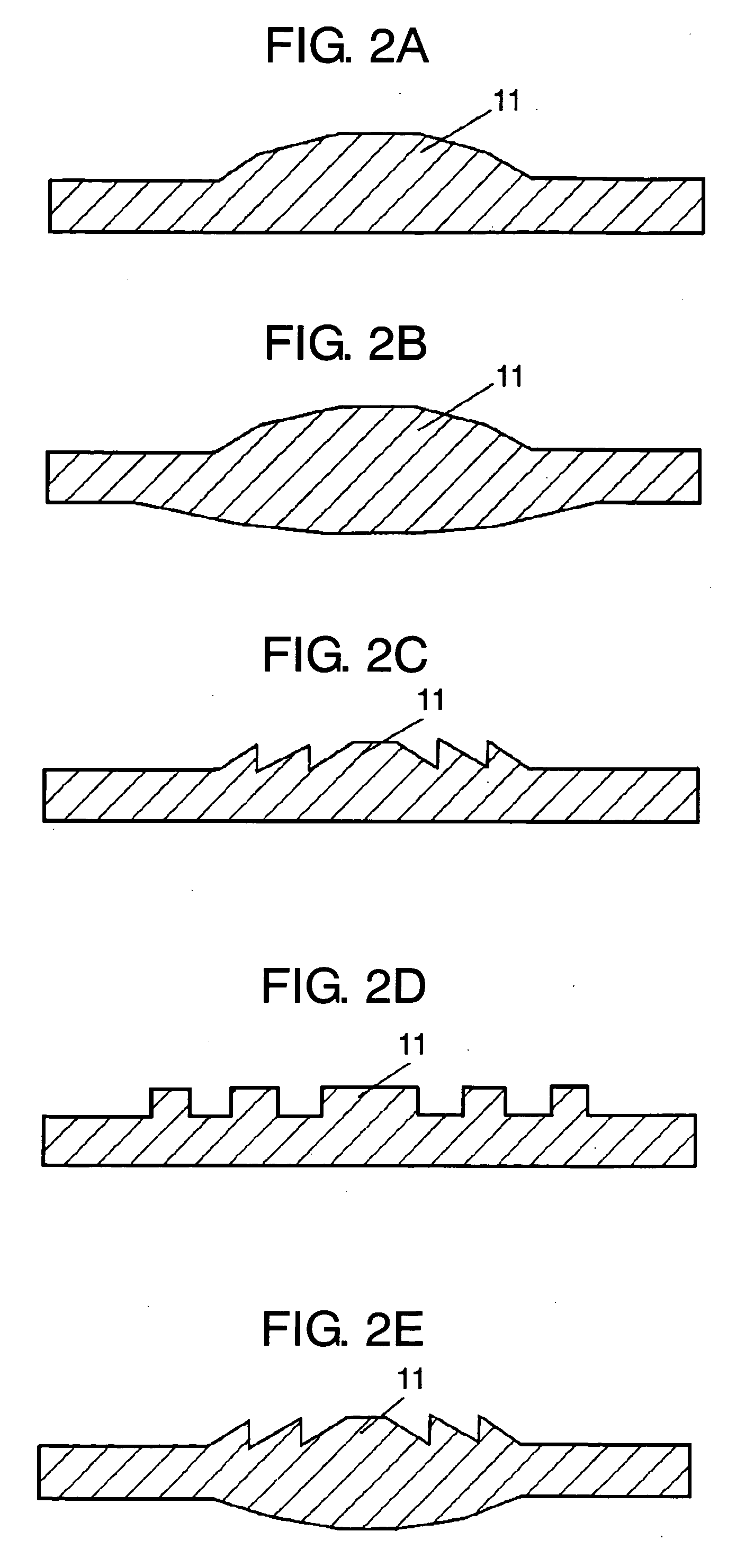
[0024]FIGS. 1A and 1B show an optical component in Embodiment 1 of the present invention. FIG. 1C shows a package in Embodiment 1 of the present invention. The optical component in Embodiment 1 includes: lens 11; cover 12 in which lens 11 is formed; concave package 13 provided by layering ceramic substrates 131; external electrode 14 provided on an outer surface of package 13; seal ring 15 fixed between package 13 and cover 12; wiring 16 provided on each layer of ceramic substrate 131; through hole electrode 17 for connecting wirings 16 provided on respective layers to one another; wire 18; groove section 19; and light-receiving element or light-emitting element (hereinafter referred to as optical semiconductor element) 20. Details of lens 11 will be described with reference to FIG. 2.

[0025] Concave package 13 is provided by layering ceramic substrates 131 having through hole electrodes 17 and wirings 16. An internal bottom face of concave package 13 includes groove section 19 havi...

embodiment 2

[0045] Next, embodiment 2 of the present invention will be described with reference to FIGS. 5A to 5D. Hereinafter, an optical component of embodiment 2 will be described according to the manufacturing steps.

[0046] As shown in FIGS. 5A to 5C, concave package 13 is provided by layering ceramic substrates 131 having through hole electrode 17 and wiring 16. In an internal bottom face of concave package 13, groove section 19 having at least two steps is provided. When groove section 19 is mounted with light-receiving element or light-emitting element (hereinafter referred to as optical semiconductor element) 20, the depth of groove section 19 is adjusted such that the internal bottom face of package 13 and a top face of optical semiconductor element 20 reach substantially the same height. Optical semiconductor element 20 is sandwiched between fixed substrate 21 having a wiring at least at the lower face and package 13. Then, an electrode of optical semiconductor element 20 is connected...


PUM


Abstract

An optical component for optical communication having a smaller size and a shorter height. The optical component involves concave package 13 provided by layering ceramic substrates 131, groove section 19 formed at a bottom face of this package 13, optical semiconductor element 20 provided in this groove section 19, cover 12 provided to cover an opening section of package 13 and lens 11 formed at cover 12.

Description

TECHNICAL FIELD [0001] The present invention relates to an optical component used for optical communication and a manufacturing method of the component. BACKGROUND OF THE INVENTION [0002] A conventional optical component used for optical communication is shown in FIGS. 7A and 7B. [0003] A light-receiving element module or a light-emitting element module shown in FIGS. 7A and 7B comprises: metallic cap 1; lens 2 bonded to metallic cap 1; metal base 3 on which a chip is mounted; external draw-out electrode 4 for connection from a main face of metal base 3 to a back face; low melting point glass 5 for hermetically sealing external draw-out electrode 4 to metal base 3; light-emitting element or light-receiving element 6 (e.g., LED, PD); and metal wire 7 for electrically connecting an electrode of element 6 to external draw-out electrode 4. [0004] As metallic cap 1 and metal base 3, an alloy such as Fe—Ni—Co having a plating of Ni—Au or the like on the surface is used for preventing the ...

Claims


Application Information

Patent Timeline
IPC IPC(8): G02B6/42G02B7/02G02B27/44H01L23/02H01L27/14H01L27/15H01L31/00H01L31/02H01L31/0232H01L33/58H01S5/022
CPCG02B6/4201G02B6/4206H01L2924/30107H01L2224/48227H01S5/183G02B7/025G02B27/4233H01L31/0203H01L31/0232H01L33/486H01L33/58H01S5/02212H01S5/02288H01L2224/48091H01L2924/00014H01L2924/00G02B6/4267G02B6/4257G02B6/4254H01L31/02325H01S5/02253
Inventor TATEHATA, NAOKINISHIHARA, KAZUNARISASHINAKA, NOBUO
Owner PANASONIC CORP
Why Eureka
Try Eureka