Method for producing semiconductor device, polishing apparatus, and polishing method
- Summary
- Abstract
- Description
- Claims
- Application Information
AI Technical Summary
Benefits of technology
Problems solved by technology
Method used
Image


Examples
modification 1
[0228] Modification 1
[0229]FIG. 26 is a schematic view of a polishing apparatus according to a modification of the present invention.
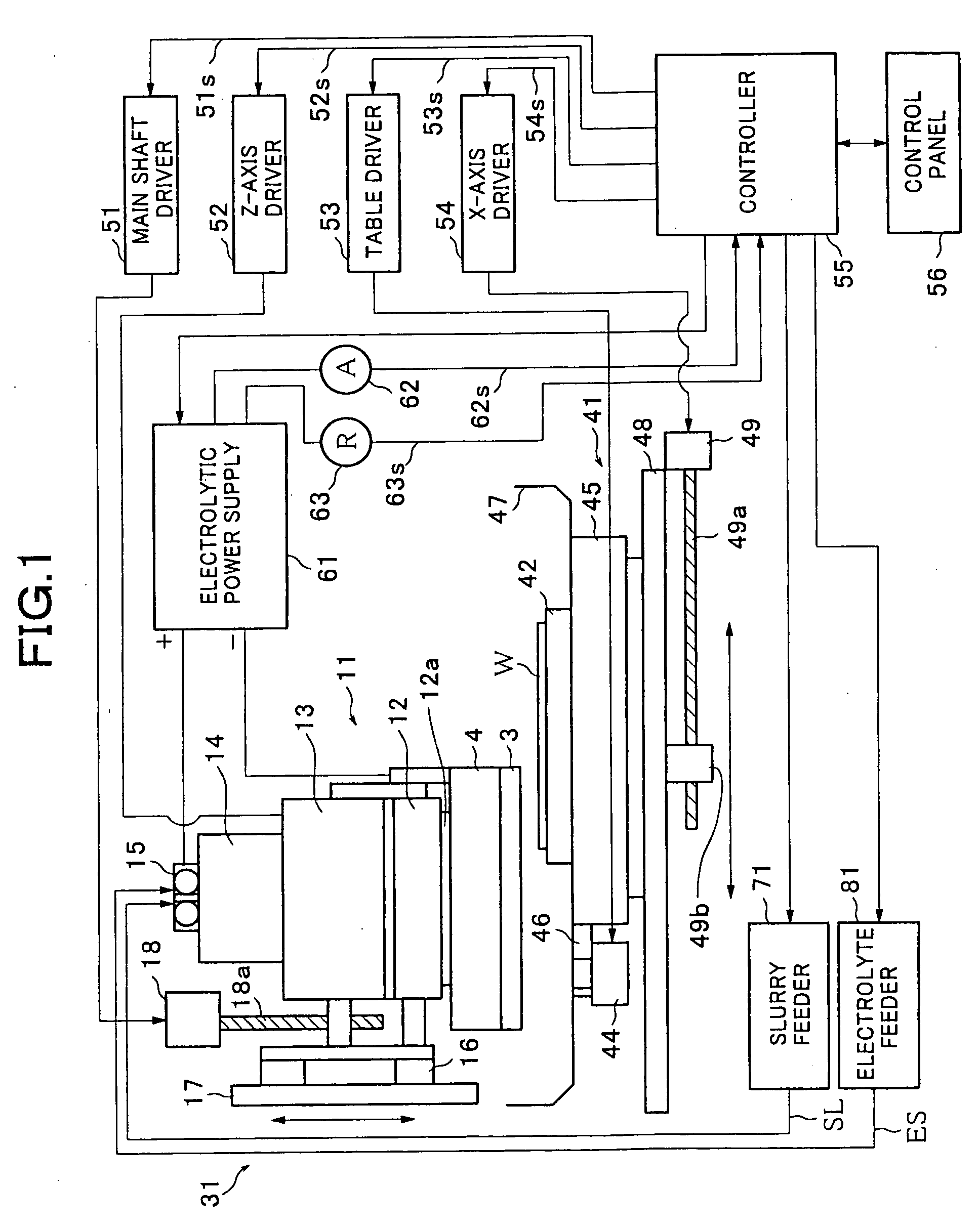
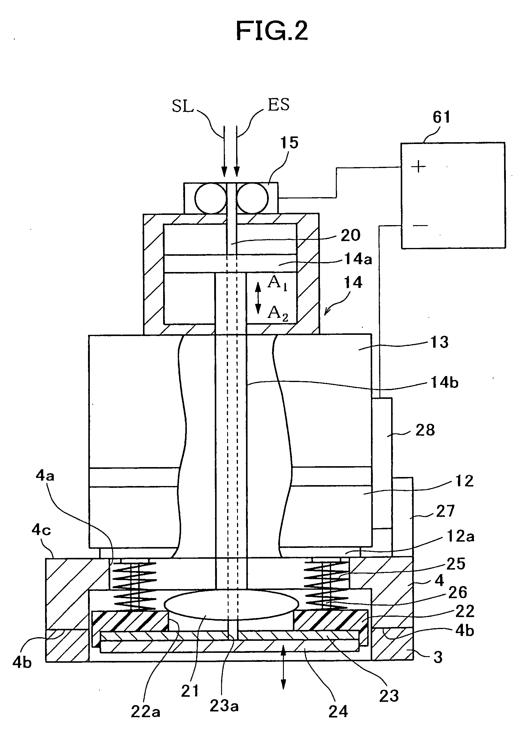
[0230] In the polishing apparatus 1 according to the embodiment mentioned above, current was conducted to the surface of the wafer W by the conductive plate 23 provided with the conductive polishing tool and the scrub member 24.
[0231] As shown in FIG. 26, it is also possible to give the wheel-like polishing tool 401 conductivity in the same way as the case of the polishing apparatus 1 and to give conductivity to a wafer table 402 for chucking and rotating the wafer W. Power is supplied to the polishing tool 401 by a configuration similar to that of the embodiments.
[0232] In this case, in supplying current to the wafer table 402, electrolytic current can be supplied by providing a rotary joint 403 below the wafer table 402 and constantly maintaining the flow of current to the wafer table 402 rotating by the rotary joint 403.
modification 2
[0233] Modification 2
[0234]FIG. 27 is a schematic view of a polishing apparatus according to another modification of the present invention.
[0235] A wafer table 502 for chucking and rotating the wafer W holds the wafer W by a retainer ring 504 provided on the periphery of the wafer W.
[0236] Conductivity is imparted to a polishing tool 501, conductivity is imparted to the retainer ring 504, and power is supplied to the polishing tool 501 by a configuration similar to that of the embodiments mentioned above.
[0237] Further, the retainer ring 504 is covered up to the barrier layer portion formed on the wafer W and supplied with current. Further, the retainer ring 504 is supplied with power through a rotary joint 503 provided below the wafer table 502.
[0238] Note that by making the amount of inclination of the polishing tool 3 larger so that a gap more than the thickness of the retainer ring 504 can be maintained at the edge portion even if the polishing tool 501 contacts the wafer W,...
modification 3
[0239] Modification 3
[0240]FIG. 28 is a schematic view of the configuration of a polishing apparatus according to another embodiment of the present invention.
[0241] The polishing apparatus shown in FIG. 28 is obtained by adding the electrolytic polishing function of the present invention to the CMP apparatus of the related art. It flattens the surface of the wafer W by bringing the entire surface of the wafer W chucked by a wafer chuck 207 into contact with the polishing surface of the polishing tool comprised of a plate 201 to which a polishing pad (polishing fabric) 202 is adhered while rotating the wafer W.
[0242] Anode electrodes 204 and cathode electrodes 203 are alternately radially arranged on the polishing pad 202. Further, the anode electrodes 204 and the cathode electrodes 203 are electrically insulated by an insulator 206, and the anode electrodes 204 and the cathode electrodes 203 are supplied with the current from the plate 201 side. The polishing pad 202 is constitute...
PUM
| Property | Measurement | Unit |
|---|---|---|
| Mechanical strength | aaaaa | aaaaa |
| Power | aaaaa | aaaaa |
| Electrical resistance | aaaaa | aaaaa |
Abstract
Description
Claims
Application Information
 - Generate Ideas
- Intellectual Property
- Life Sciences
- Materials
- Tech Scout
- Unparalleled Data Quality
- Higher Quality Content
- 60% Fewer Hallucinations
Browse by: Latest US Patents, China's latest patents, Technical Efficacy Thesaurus, Application Domain, Technology Topic, Popular Technical Reports.
© 2025 PatSnap. All rights reserved.Legal|Privacy policy|Modern Slavery Act Transparency Statement|Sitemap|About US| Contact US: help@patsnap.com