

Cleaning method and system of semiconductor substrate and production method of cleaning solution
a cleaning method and cleaning system technology, applied in the direction of cleaning using liquids, water/sewage treatment by ion exchange, water/sewage treatment, etc., can solve the problems of property or performance degradation of semiconductor devices, high concentration of chemicals significantly affecting the earth environment, and high cost of producing these chemicals and disposing of waste generated therefrom
- Summary
- Abstract
- Description
- Claims
- Application Information
AI Technical Summary
Benefits of technology
Problems solved by technology
Method used
Image

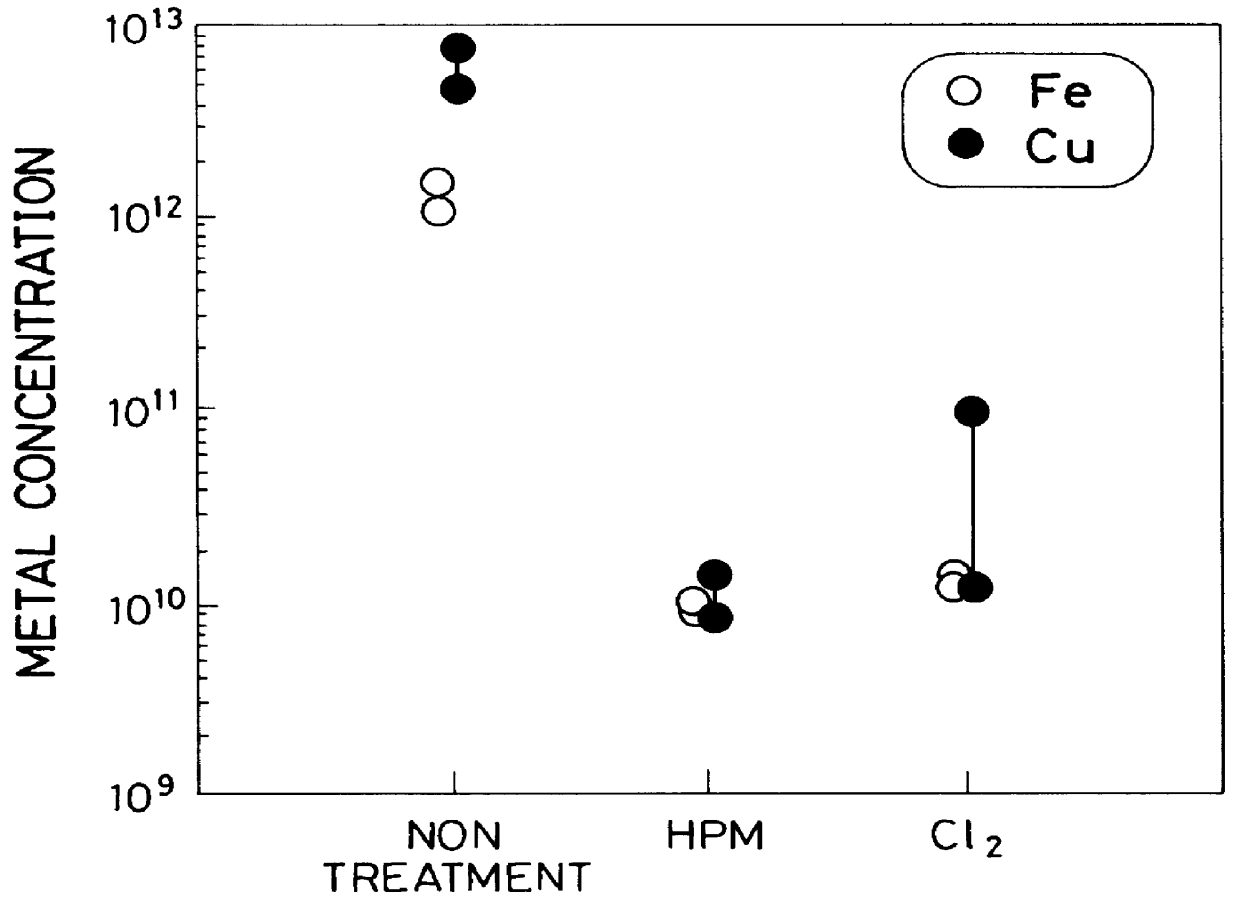
Examples
first embodiment
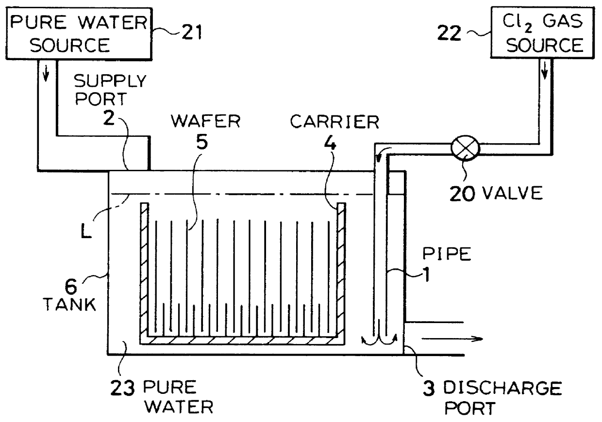
Next, a cleaning method of a semiconductor substrate is explained.
First, after opening the supply port 2 and closing the discharge port 3, the pure water 23 is supplied to the cleaning tank 6 from the pure water source 21 until the top level L of the water 23 reaches a specified height from the bottom of the tank 6. Then, the supply port 2 is closed.
Next, a Cl.sub.2 gas is supplied from the Cl.sub.2 gas source 22 to the pure water 23 existing in the tank 6 through the pipe 1. The Cl.sub.2 gas is bubbled into the water 23 through the open end of the pipe 1 to be dissolved therein. Thus, chlorine ions (Cl.sup.-), hypochlorite ions (ClO.sup.-), chlorite ions (ClO.sub.2.sup.-), and chlorate ions (ClO.sub.3.sup.-) are generated in the water 23.
The amount of the dissolved chlorine in the pure water 23 is controlled to be in the range from 0.003 to 0.3% by weight by adjusting the valve 20 provided in the pipe 1.
Subsequently, the wafer carrier 4 holding the semiconductor wafers 5 thereon i...
second embodiment
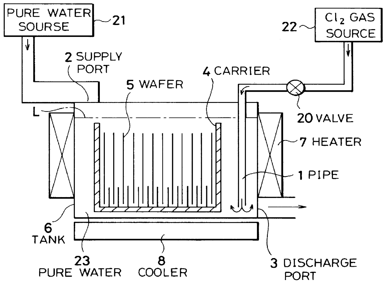
A cleaning system of a semiconductor substrate shown in FIG. 3 is used for a cleaning method according to a second embodiment. This system has the same structure as that of the first embodiment except for a heater 7 and a cooler 8. Accordingly, the explanation relating to the same structure is omitted here by attaching the same reference numerals to the corresponding elements for the sake of simplification of description.
The heater 7 is fixed near the side wall of the cleaning tank 6, and is used for raising the temperature of the pure water 23 in the tank 6. Here, the heater 7 is made of a microwave oscillator to realize a rapid heating.
The cooler 8 is fixed near the bottom wall of the tank 6, and is used for lowering the temperature of the pure water 23 in the tank 6.
The cleaning solution (i.e., the pure water 23 containing the Cl.sup.-, ClO.sup.-, ClO.sub.2.sup.- and ClO.sub.3.sup.-) becomes more active as the temperature of the solution increases. In other words, the decompositi...
third embodiment
A cleaning system of a semiconductor substrate shown in FIG. 5 is used for a cleaning method according to a third embodiment. This system has the same structure as that of the first embodiment except that a cleaning tank 6A made of high-purity quartz is provided and that a plurality of UV lamps 9 are provided near the side and bottom walls of the tank 6A. Accordingly, the explanation relating to the same structure is omitted by attaching the same reference numerals to the corresponding elements for the sake of simplification.
The UV lamps 9 are used for generating and irradiating UV light (the wavelength of which is 200 to 300 nm) to the cleaning solution.
The cleaning solution becomes more active due to UV light irradiation and accordingly, the decomposition of the hypochlorous acid ions is promoted by the applied light according to the above equation.
Therefore, if the Uw light is irradiated to the solution by the operation of the lamps 9 during the process step of immersing the wafe...
PUM
| Property | Measurement | Unit |
|---|---|---|
| Oxidation Reduction Potential | aaaaa | aaaaa |
| Oxidation Reduction Potential | aaaaa | aaaaa |
| oxidation reduction potential | aaaaa | aaaaa |
Abstract
Description
Claims
Application Information