

Methods of producing and polishing semiconductor device and polishing apparatus
- Summary
- Abstract
- Description
- Claims
- Application Information
AI Technical Summary
Benefits of technology
Problems solved by technology
Method used
Image

Examples
first embodiment
[0121]A description will be made of embodiments of the present invention by taking as an example the case where the present invention is applied to a process of formation of metal interconnections by a dual damascene process in a method of production of a semiconductor device.
[0122]Polishing Method
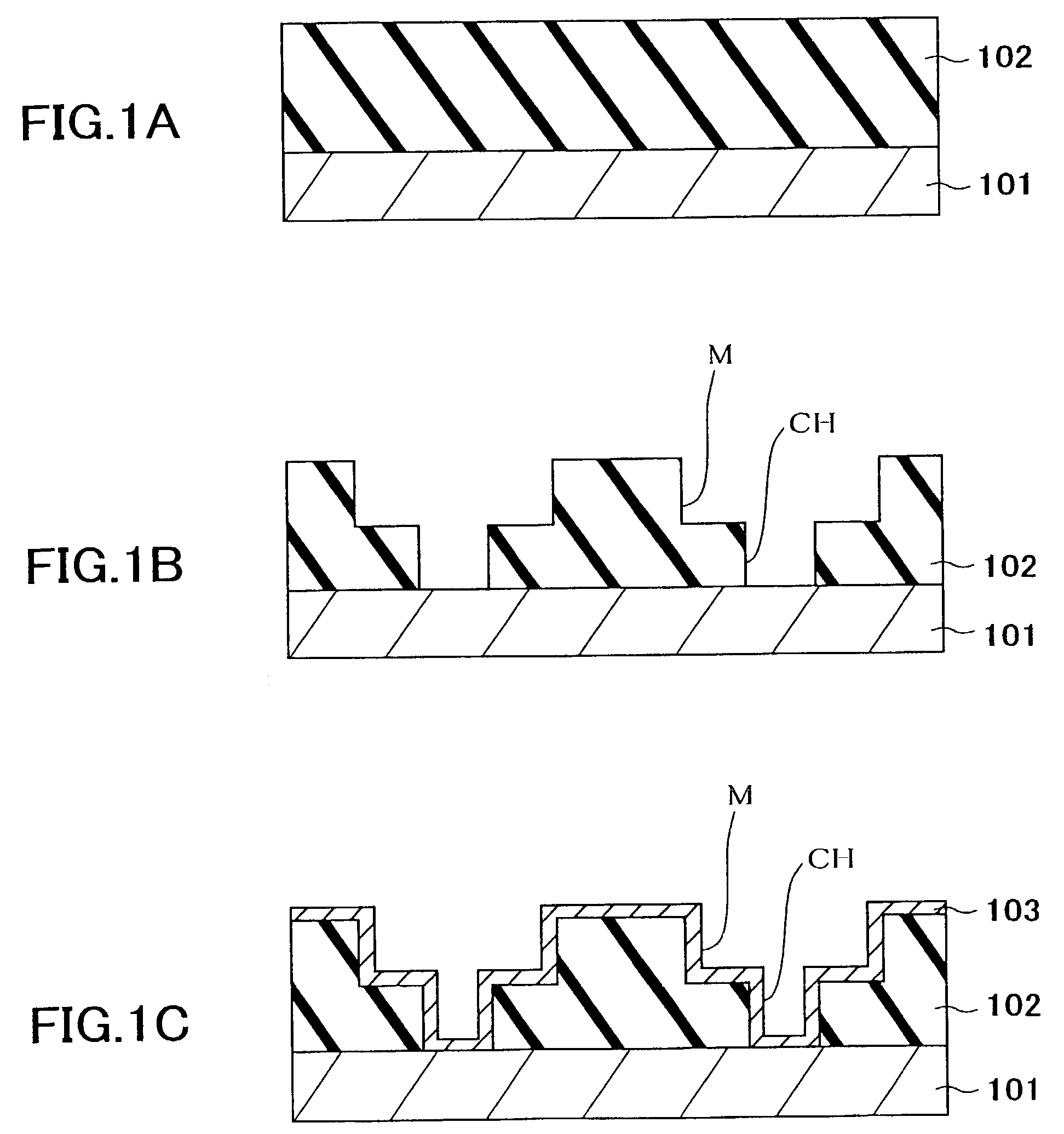
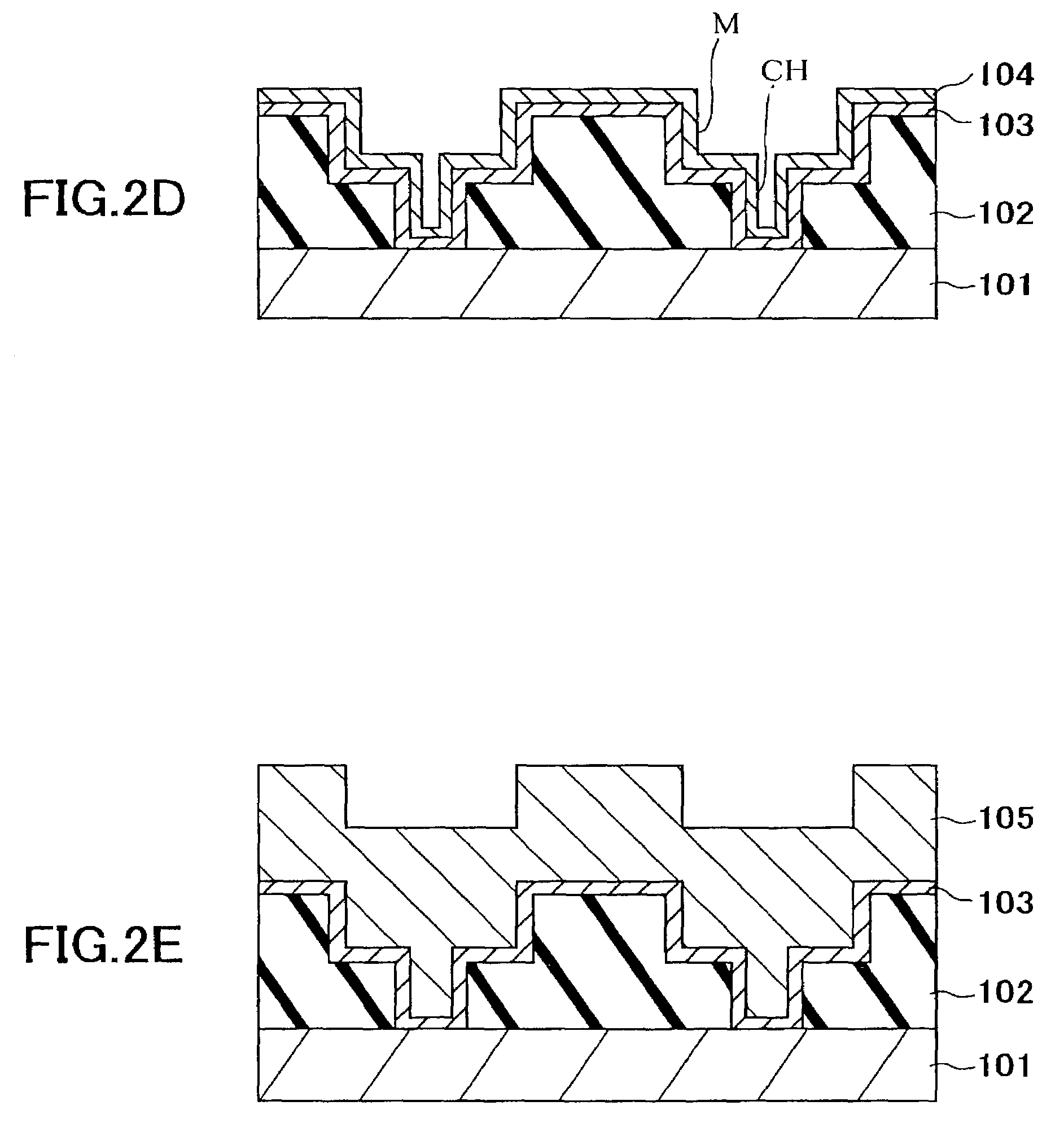
[0123]First, as shown in FIG. 1A, for example an interlayer insulation film 102 made of for example a silicon oxide film (SiO2) is formed by a low pressure chemical vapor deposition (LP-CVD) process by using for example tetraethyl orthosilicate (TEOS) as the reaction source on a silicon or other semiconductor substrate 101 on which a not illustrated impurity diffusion region or an interconnection is suitably formed.
[0124]Note that as the interlayer insulation film 102, use can be made of a so-called low-k (low dielectric constant) material, in addition to a TEOS (tetraethyl orthosilicate) film and a silicon nitride film formed by a CVD process.
[0125]Here, the low dielectric constant materi...
second embodiment
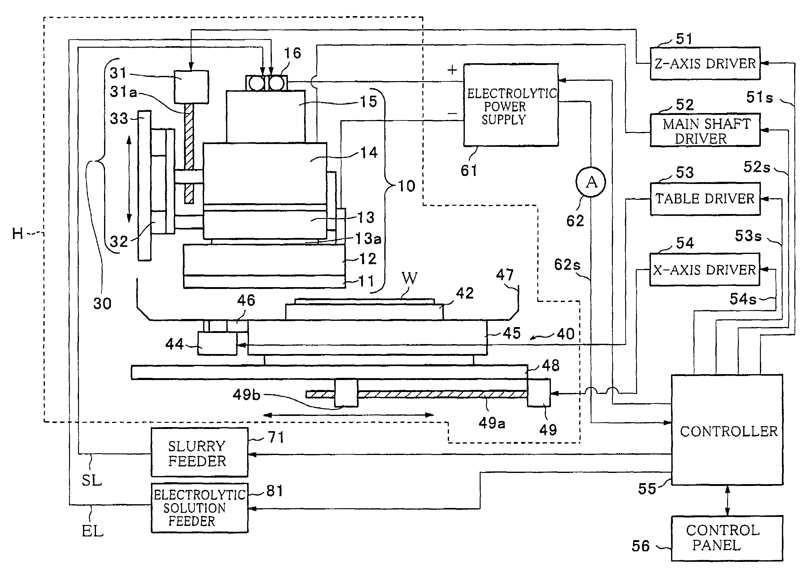
[0276]FIG. 19 is a schematic view of the configuration of a polishing apparatus according to a second embodiment of the present invention. The polishing apparatus according to the present embodiment comprises a tank 501 filled with a predetermined amount of electrolytic solution EL, a wafer holding means 530 and an electrode plate 510 arranged in the electrolytic solution EL in the tank, a jet pump 520 (flowing means) for sucking the electrolytic solution EL in the tank using a tube 522 and ejecting the same as a jet using a tube 521, a power supply 561 (electrolytic current supplying means) for applying a voltage using the electrode plate 510 as a cathode and a wafer as an anode, an ammeter 562, a controller 555, and a control panel 556.
[0277]The holding means 530 comprises a first holding member 531 and a second holding member 532 having conductivity and for holding a wafer and a Z-axis positioning mechanism fixed to a not illustrated column and for fixing the first holding member...
third embodiment
[0293]FIG. 20 is a schematic view of the configuration of a polishing apparatus according to a third embodiment of the present invention. The polishing apparatus according to the present embodiment comprises a vibration applying means including a pulse generator 640, an amplifier 641, and an oscillator 643, a tank 601 filled with a predetermined amount of electrolytic solution EL, a wafer holding means 630 and an electrode plate 610 arranged in the electrolytic solution EL in the tank, a power supply 661 (electrolytic current supplying means) for applying a voltage using the electrode plate 610 as a cathode and a wafer as an anode, an ammeter 662, a controller 655, and a control panel 656.
[0294]The holding means 630 comprises a first holding member 631 for holding the electrode plate to be parallel with the wafer W, a second holding member 632 and a third holding member 633 for pressing and fixing the wafer between them, and a fourth holding member 634 with one end attached to the s...
PUM
| Property | Measurement | Unit |
|---|---|---|
| Temperature | aaaaa | aaaaa |
| Current | aaaaa | aaaaa |
| Electric potential / voltage | aaaaa | aaaaa |
Abstract
Description
Claims
Application Information