
Method for producing semiconductor device, polishing apparatus, and polishing method

a technology of polishing apparatus and semiconductor, applied in the direction of lapping machines, manufacturing tools, transistors, etc., can solve the problems of poor interconnection resistance, insufficient sectional area of interconnections, poor interconnection resistance, etc., and achieve the effect of high efficiency removal and high efficiency removal

Inactive Publication Date: 2007-06-19
SONY CORP
View PDF1 Cites 3 Cited by
  • Summary
  • Abstract
  • Description
  • Claims
  • Application Information

AI Technical Summary

Benefits of technology

The present invention provides a polishing apparatus and method for flattening unevenness in a metal film of a semiconductor device. The apparatus includes a polishing tool with conductivity, a rotating and holding means for the polishing tool, a movement and positioning means for the polishing tool, an electrolyte feeding means, an electrolytic current supplying means, and a polishing method using electrolytic composite polishing. The apparatus and method can efficiently flatten the metal film and remove excess metal film while preventing damage to the underlying layers. The invention also provides a method for producing a semiconductor device by forming an interconnection use groove, stacking a metal film on the insulation film, selectively removing a passivation film on a projecting portion, and using electrolytic polishing and mechanical polishing to flatten the surface and remove excess metal film.

Problems solved by technology

This becomes a cause of poor interconnection resistance etc.
When erosion occurs, the sectional area of the interconnections becomes insufficient.
This becomes a cause of poor interconnection resistance etc.
In this case as well, the sectional area of the interconnections becomes insufficient.
This becomes a cause of poor interconnection resistance etc.
For this reason, it becomes a cause of opening of the interconnections, short-circuiting, poor interconnection resistance, and other disadvantages.
Further, if the polishing pressure is raised, there is the inconvenience that the amount of the occurrence of dishing, erosion, and recesses becomes larger.

Method used


Image

  • Method for producing semiconductor device, polishing apparatus, and polishing method
  • Method for producing semiconductor device, polishing apparatus, and polishing method
  • Method for producing semiconductor device, polishing apparatus, and polishing method

Examples


modification 1

[0229

[0230]FIG. 26 is a schematic view of a polishing apparatus according to a modification of the present invention.

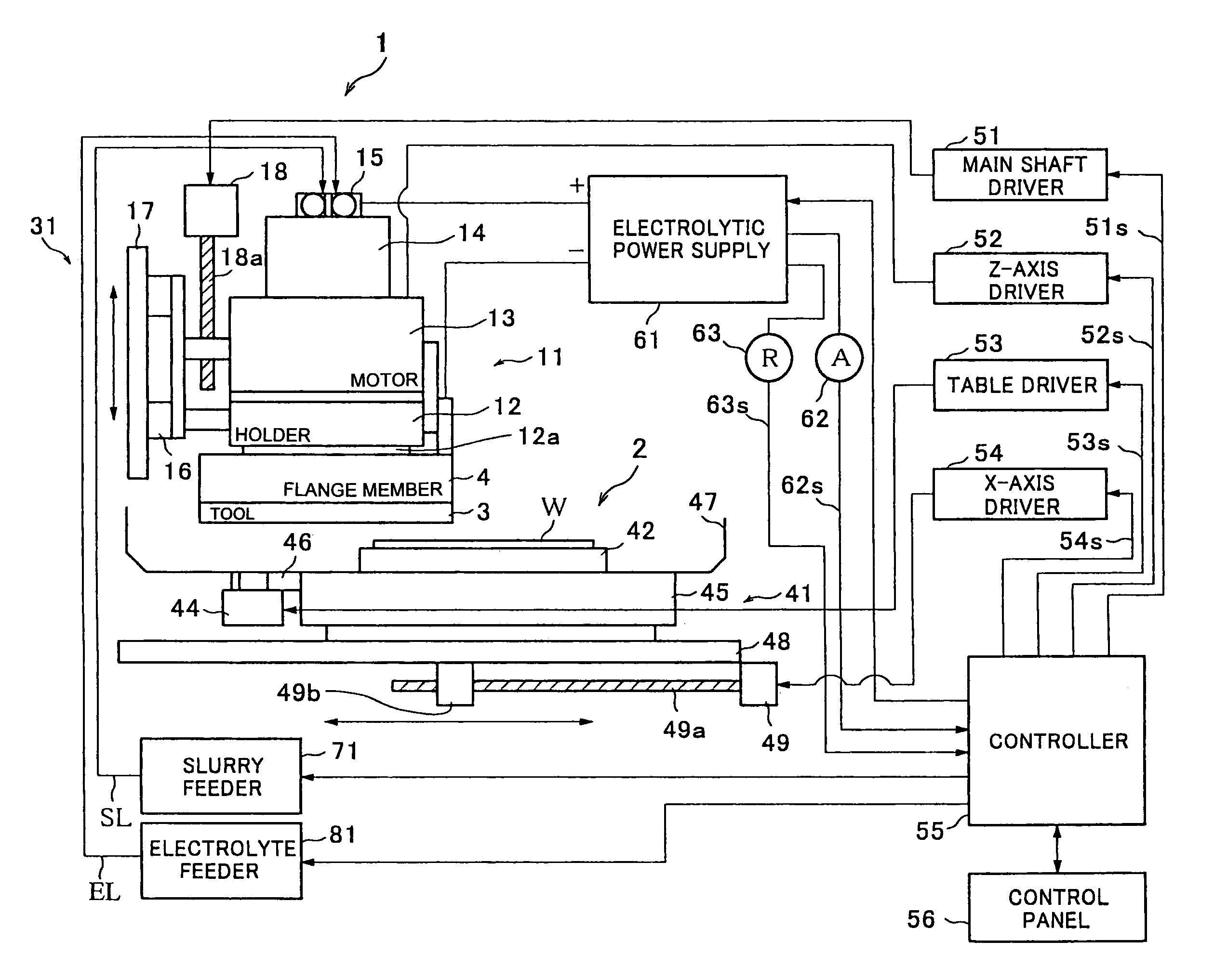
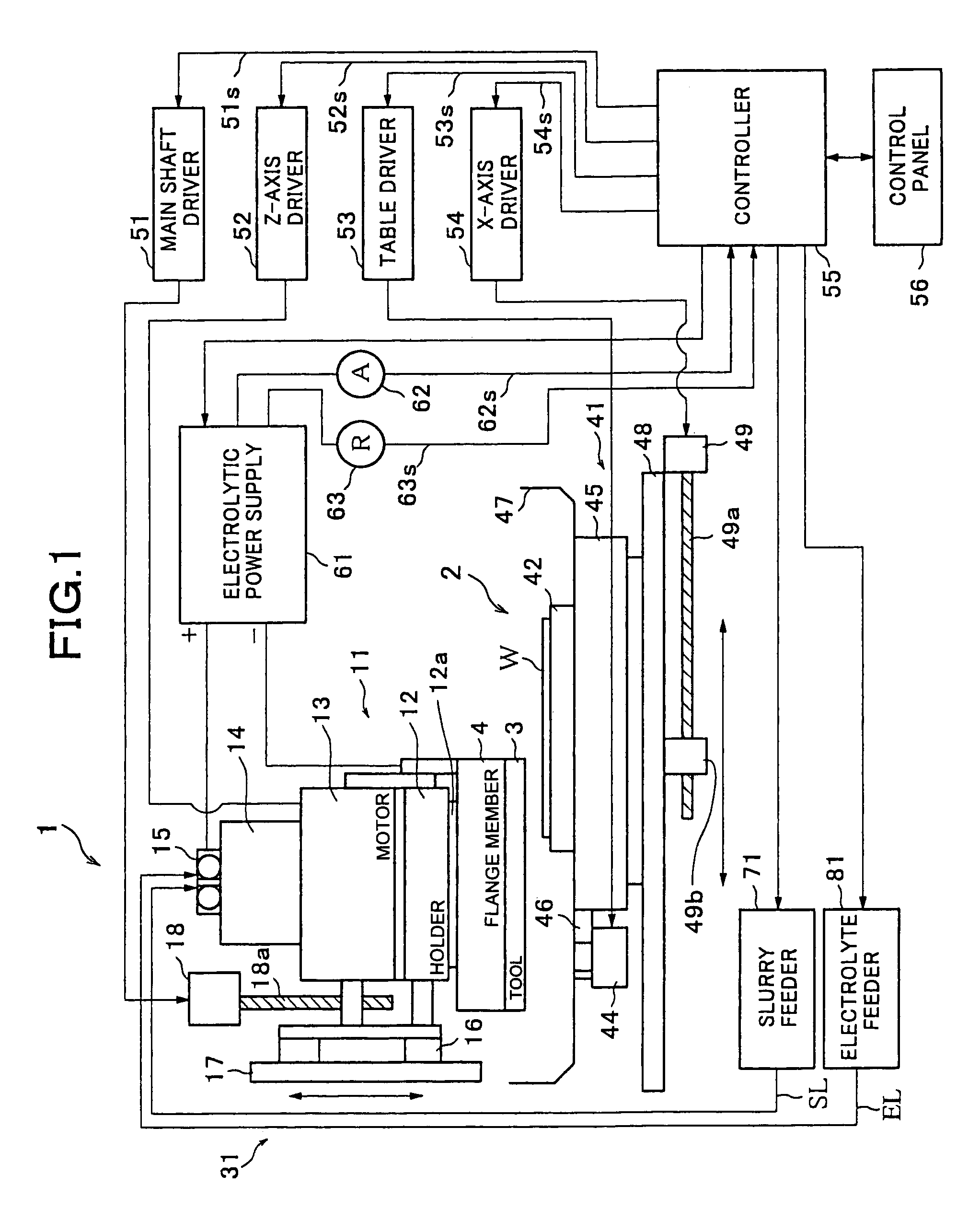
[0231]In the polishing apparatus 1 according to the embodiment mentioned above, current was conducted to the surface of the wafer W by the conductive plate 23 provided with the conductive polishing tool and the scrub member 24.

[0232]As shown in FIG. 26, it is also possible to give the wheel-like polishing tool 401 conductivity in the same way as the case of the polishing apparatus 1 and to give conductivity to a wafer table 402 for chucking and rotating the wafer W. Power is supplied to the polishing tool 401 by a configuration similar to that of the embodiments.

[0233]In this case, in supplying current to the wafer table 402, electrolytic current can be supplied by providing a rotary joint 403 below the wafer table 402 and constantly maintaining the flow of current to the wafer table 402 rotating by the rotary joint 403.

modification 2

[0234

[0235]FIG. 27 is a schematic view of a polishing apparatus according to another modification of the present invention.

[0236]A wafer table 502 for chucking and rotating the wafer W holds the wafer W by a retainer ring 504 provided on the periphery of the wafer W.

[0237]Conductivity is imparted to a polishing tool 501, conductivity is imparted to the retainer ring 504, and power is supplied to the polishing tool 501 by a configuration similar to that of the embodiments mentioned above.

[0238]Further, the retainer ring 504 is covered up to the barrier layer portion formed on the wafer W and supplied with current. Further, the retainer ring 504 is supplied with power through a rotary joint 503 provided below the wafer table 502.

[0239]Note that by making the amount of inclination of the polishing tool 3 larger so that a gap more than the thickness of the retainer ring 504 can be maintained at the edge portion even if the polishing tool 501 contacts the wafer W, interference between th...

modification 3

[0240

[0241]FIG. 28 is a schematic view of the configuration of a polishing apparatus according to another embodiment of the present invention.

[0242]The polishing apparatus shown in FIG. 28 is obtained by adding the electrolytic polishing function of the present invention to the CMP apparatus of the related art. It flattens the surface of the wafer W by bringing the entire surface of the wafer W chucked by a wafer chuck 207 into contact with the polishing surface of the polishing tool comprised of a plate 201 to which a polishing pad (polishing fabric) 202 is adhered while rotating the wafer W.

[0243]Anode electrodes 204 and cathode electrodes 203 are alternately radially arranged on the polishing pad 202. Further, the anode electrodes 204 and the cathode electrodes 203 are electrically insulated by an insulator 206, and the anode electrodes 204 and the cathode electrodes 203 are supplied with the current from the plate 201 side. The polishing pad 202 is constituted by these anode ele...


PUM

PropertyMeasurementUnit
widthaaaaaaaaaa
widthaaaaaaaaaa
widthaaaaaaaaaa

Abstract

A method for producing a semiconductor device, polishing method, and polishing apparatus, suppressing occurrence of dishing and erosion in a flattening process by polishing of a metal film for constituting an interconnection of a semiconductor device having a multilayer interconnection structure. The production method includes the steps of: forming a passivation film exhibiting an action of inhibiting an electrolytic reaction of a metal at the surface of the metal film; selectively removing the passivation film on a projecting portion so as to expose the projecting portion of the metal film at the surface; removing the exposed projecting portion of the metal film by electrolytic polishing so as to flatten unevenness of the surface of the metal film; and removing the metal film present on an insulation film from the metal film with the flattened surface by electrolytic composite polishing combining electrolytic polishing and mechanical polishing so as to form an interconnection.

Description

RELATED APPLICATION[0001]This application is a continuation of application Ser. No. 09 / 655,833 filed on Sep. 6, 2000 now U.S. Pat. No. 6,693,036.BACKGROUND OF THE INVENTION[0002]1. Field of the Invention[0003]The present invention relates to a polishing apparatus and a polishing method for flattening an uneven surface accompanying for example a multilayer interconnection structure of a semiconductor device and a method for producing a semiconductor device having a multilayer interconnection structure.[0004]2. Description of the Related Art[0005]Along with the increase in integration and reduction of size of semiconductor devices, progress has been made in miniaturization of interconnections, reduction of interconnection pitch, and superposition of interconnections. The importance of the multilayer interconnection technology in the manufacturing process of semiconductor devices is therefore rising.[0006]On the other hand, conventionally aluminum (Al) has been frequently used as an in...

Claims


Application Information

Patent Timeline
Patent Type & Authority Patents(United States)
IPC IPC(8): H01L21/302H01L21/461H01L21/3205B24B37/04H01L21/304H01L21/3063H01L21/321H01L21/336H01L21/768H01L29/78H01L29/786
CPCB24B37/042B24B37/046H01L21/32125H01L21/7684H01L21/302
Inventor NOGAMI, TAKESHIYOSHIO, AKIRASATO, SHUZO
Owner SONY CORP
Features
  • Generate Ideas
  • Intellectual Property
  • Life Sciences
  • Materials
  • Tech Scout
  • Unparalleled Data Quality
  • Higher Quality Content
  • 60% Fewer Hallucinations
Learn More