
Super-junction semiconductor device and method of manufacturing the same

a super-junction, semiconductor technology, applied in the direction of semiconductor devices, electrical appliances, transistors, etc., can solve the problems of high on-resistance and loss increase, failure, and inability to meet the requirements of the peripheral region, and achieve the effect of facilitating the provision of the peripheral region

Inactive Publication Date: 2005-01-27
FUJI ELECTRIC SYST CO LTD
View PDF21 Cites 31 Cited by
  • Summary
  • Abstract
  • Description
  • Claims
  • Application Information

AI Technical Summary

Benefits of technology

[0010] It is an object of the present invention to provide a super-junction semiconductor device that facilitates providing the peripheral region thereof with a breakdown voltage higher than the breakdown voltage in the drain drift layer without employing a guard ring or field plate.

Problems solved by technology

Therefore, breakdown is caused before the voltage between the drain and the source reaches the designed breakdown voltage of the device.
However, a thick n−-type drain drift layer 12 inevitably causes high on-resistance and loss increase.
It is difficult, however, to optimize the integral structure integrating the alternating conductivity type drain drift layer 22 for obtaining a higher breakdown voltage and the conventional guard ring or the conventional field plate for obtaining a certain local breakdown voltage in the peripheral region of the device.
In other words, it is difficult to correct the depletion electric field by an external means added from outside such as the integral structures described above.
The reliability of semiconductor device having such an external means for correcting depletion electric field is not high.
Therefore, the conventional guard or the conventional field plate is not effective to provide the entire device structure with a high breakdown voltage nor to fully utilize the functions of the alternating conductivity type drain drift layer.

Method used


Image

  • Super-junction semiconductor device and method of manufacturing the same
  • Super-junction semiconductor device and method of manufacturing the same
  • Super-junction semiconductor device and method of manufacturing the same

Examples


first embodiment

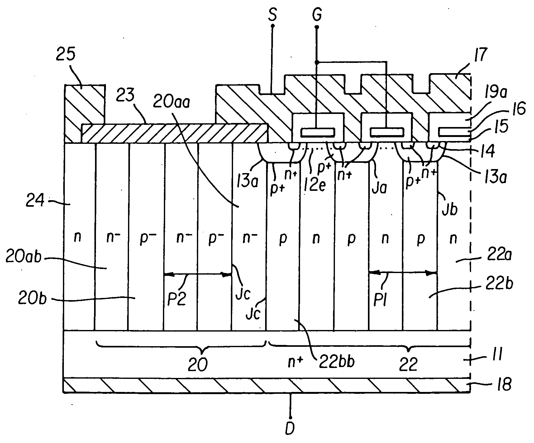
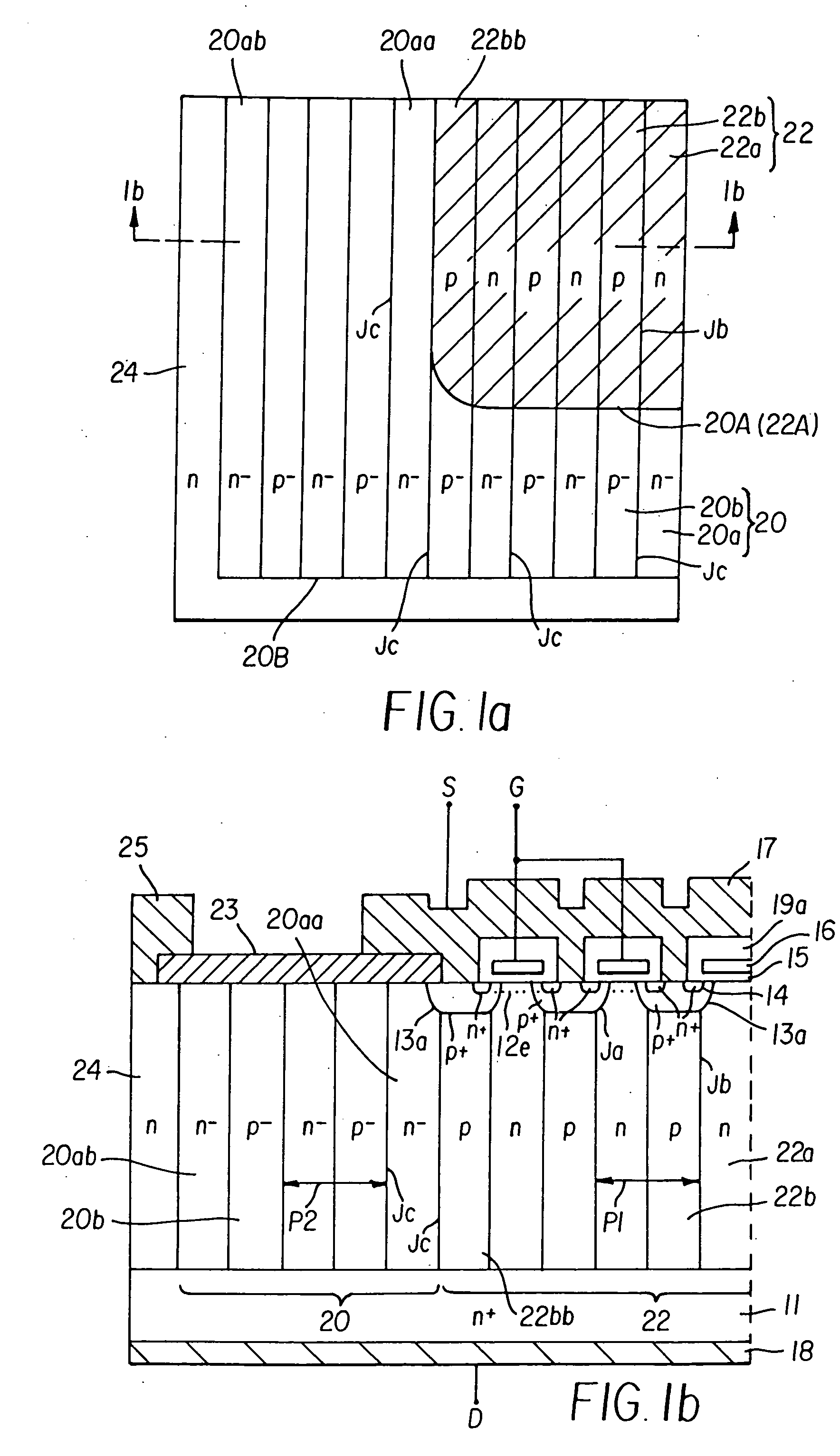
[0050]FIG. 1(a) is a horizontal cross sectional view showing a drain drift region and a breakdown withstanding region of a vertical super-junction MOSFET according to a first embodiment of the invention. FIG. 1(b) is the vertical cross sectional view along 1(b)-1(b) of FIG. 1(a). In FIG. 1(a), a quarter part of the drain drift region is illustrated by hatching. In these figures, the alternating conductivity type layers are mainly illustrated for the ease of understanding.

[0051] Referring to FIG. 1(b), the n-channel vertical MOSFET includes an n+-type drain layer (n+-type drain contact layer) 11; a drain electrode 18 in electrical contact with n+ drain layer 11; a drain drift region 22 including a first alternating conductivity type layer on n+ drain layer 11; heavily doped p-type base regions (p-type well region) 13a, which constitute an active region of the device, formed selectively in the surface portion of drain drift region 22; a heavily doped n+-type source region 14 formed s...

second embodiment

[0093]FIG. 4(a) is a horizontal cross sectional view showing a drain drift region and a breakdown withstanding region of a vertical super-junction MOSFET according to a second embodiment of the invention. FIG. 4(b) is the vertical cross sectional view along 4(b)-4(b) of FIG. 4(a). In FIG. 4(a), a quarter part of the drain drift region is illustrated by hatching. In FIGS. 4(a) and 4(b), the same reference numerals as used in FIGS. 1(a) and 1(b) are used to designate the same constituent elements and their duplicated explanations are omitted for clarity.

[0094] The MOSFET shown in FIGS. 4(a) and 4(b) is different from the MOSFET shown in FIGS. 1(a) and 1(b) in that the pitch of repeating P2, at that a pair of n− region 20a and p− region 20b is repeated in a breakdown withstanding region 120 is wider than the pitch of repeating P1, at that a pair of n drift current path region 22a and p partition region 22b in drain drift region 22 is repeated in drain drift region 22. Since the impuri...

third embodiment

[0110]FIG. 6 is a horizontal cross sectional view showing a drain drift region and a breakdown withstanding region of a vertical super-junction MOSFET according to a third embodiment of the invention. FIG. 7 is the vertical cross sectional view along 7-7 of FIG. 6. In FIG. 6, a quarter part of the drain drift region is illustrated by hatching. In FIGS. 6 and 7, the same reference numerals as used in FIGS. 1(a) and 1(b) are used to designate the same constituent elements and their duplicated explanations are omitted for clarity.

[0111] The MOSFET shown in FIGS. 6 and 7 is different from the MOSFET shown in FIGS. 1(a) and 1(b) in that the pitch of repeating P2, at that a pair of n− region 20a and p− region 20b is repeated in a breakdown withstanding region 220 is narrower than the pitch of repeating P1, at that a pair of n drift current path region 22a and p partition region 22b in drain drift region 22 is repeated in drain drift region 22, in that the impurity concentration in the se...


PUM


Abstract

Disclosed is a semiconductor device facilitating a peripheral portion thereof with a breakdown voltage higher than the breakdown voltage in the drain drift layer without employing a guard ring or field plate. A preferred embodiment includes a drain drift region with a first alternating conductivity type layer formed of n drift current path regions and p partition regions arranged alternately with each other, and a breakdown withstanding region with a second alternating conductivity type layer formed of n regions and p regions arranged alternately with each other, the breakdown withstanding region providing no current path in the ON-state of the device and being depleted in the OFF-state of the device. Since depletion layers expand in both directions from multiple pn-junctions into n regions and p regions in the OFF-state of the device, the adjacent areas of p-type base regions, the outer area of the semiconductor chip and the deep area of the semiconductor chip are depleted. Thus, the breakdown voltage of breakdown withstanding region is higher than the breakdown voltage of drain drift region.

Description

FIELD OF THE INVENTION [0001] The present invention relates to vertical power semiconductor devices that facilitate a high breakdown voltage and a high current capacity, such as MOSFET (insulated gate field effect transistors), IGBT (conductivity-modulation-type MOSFET), bipolar transistors and diodes. The present invention relates also to the method of manufacturing such semiconductor devices. DESCRIPTION OF RELATED ART [0002] Semiconductor devices may be roughly classified as lateral devices that arrange electrodes on a major surface, or vertical devices that distribute electrodes on both major surfaces facing opposite to each other. When a vertical semiconductor device is ON, a drift current flows in the thickness direction of the semiconductor chip (vertical direction). When the vertical semiconductor device is OFF, the depletion layers caused by applying a reverse bias voltage expand also in the vertical direction. [0003]FIG. 28 is a cross sectional view of a conventional plana...

Claims


Application Information

Patent Timeline
IPC IPC(8): H01L21/331H01L29/06H01L21/336H01L29/739H01L29/78H01L29/861
CPCH01L29/0619H01L29/0634H01L29/0696H01L29/66333H01L29/66712H01L2924/0002H01L29/7395H01L29/7802H01L2924/00H01L29/7811
Inventor ONISHI, YASUHIKOFUJIHIRA, TATSUHIKOUENO, KATSUNORIIWAMOTO, SUSUMUSATO, TAKAHIRONAGAOKA, TATSUJI
Owner FUJI ELECTRIC SYST CO LTD
Learn More