
System and method for derivative-free optimization of electrical circuits

a derivative-free, electrical circuit technology, applied in the field of electrical circuit design, can solve the problems of not possessing any guarantee of convergence to even a local optimum, requiring a large number of computationally intensive circuit simulations, and the inability of nelder and mead algorithm in certain circumstances to solve, so as to improve the understanding of the tradeoffs inherent in the circuit, improve the design quality, and improve the effect of designer productivity

Inactive Publication Date: 2005-01-27
IBM CORP
View PDF2 Cites 16 Cited by
  • Summary
  • Abstract
  • Description
  • Claims
  • Application Information

AI Technical Summary

Benefits of technology

The present invention is a system and method for optimizing electrical circuits by means of derivative-free optimization. Tunable parameters such as component values, transistor sizes or model parameters are automatically adjusted to obtain an optimal circuit. Any method of measuring the performance of the circuit, including computer simulation, can be incorporated into the optimization technique, with no derivative requirements. An arbitrary continuous optimization problem can be posed, including an objective function, equality and inequality constraints, and simple bounds on the tunable parameters. The optimization technique is efficient and guarantees that it will find a locally optimal solution from any starting point. Further, the procedure includes a method of automatically recovering from electrical failure to enable automatic and productive circuit optimization. A set of measurement widgets is provided to automatically introduce the checking required to recover from electrical failure. The automated circuit optimization leads to higher quality circuits, increases designer productivity, results in a better understanding of the tradeoffs inherent in the circuit and lifts the thinking of the circuit designer to a higher level.

Problems solved by technology

These methods do not possess any guarantee of convergence to even a local optimum, and can require a very large number of computationally intensive circuit simulations to obtain a result.
In fact, it can be shown that the Nelder and Mead algorithm is incapable in certain circumstances of solving even a 2-variable unconstrained convex minimization problem.
Thus, this category of techniques suffers from long run times, often poor quality of results and the lack of a guarantee of optimality.
Unfortunately, if there are n tunable parameters, each iteration of the optimization would require at least (n+1) simulations of the underlying circuit, one simulation to determine the objective function and constraint values, and n simulations in each of which one tunable parameter is perturbed by a small amount.
Unfortunately, this second set of techniques suffers from several problems.
First, the number of simulations of the circuit quickly grows excessive and therefore the computer run time of the overall optimization is prohibitive.
Second, these techniques suffer from numerical problems.
The resulting measurements from all simulation programs suffer from numerical noise, because of finite-precision arithmetic on a computer, because of tolerances used to judge the convergence of iterative techniques within the simulator, and because of discretizations used in the simulator models.
So, if the amount of perturbation used in the finite differencing is too small, the derivative obtained may be noisy or even incorrect, leading to increased computer time or even non-convergence in the overall optimization.
However, if the amount of the perturbation used in the finite differencing is too large, the derivatives are inaccurate and can lead to the same type of problems.
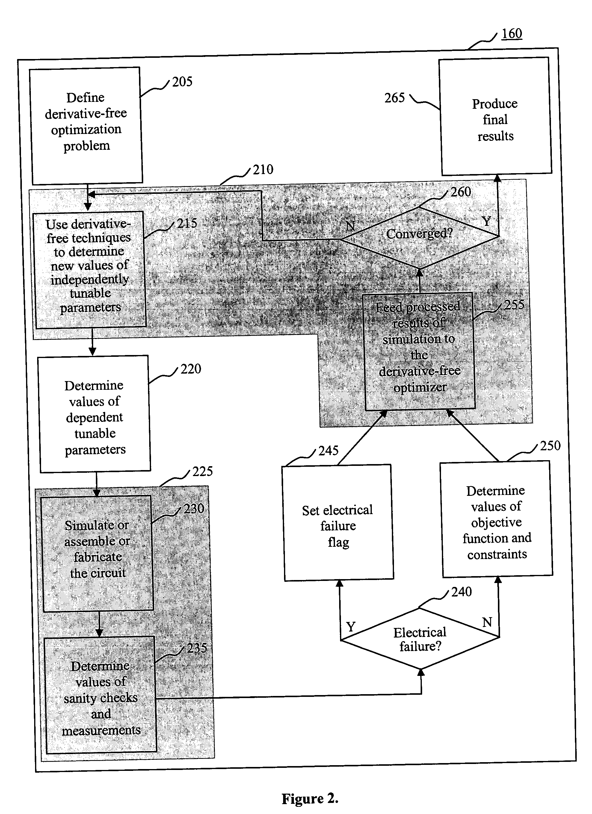
Both sets of techniques suffer from another insidious problem—that of “electrical failure.” For example, assume that the goal of the optimization is to minimize the time at which a certain digital signal switches from a low voltage to a high voltage.
In this case, there is no way of measuring the switching time, and this type of situation is referred to as electrical failure.
In a derivative-free context, electrical failure is common and causes the optimization procedure to grind to a halt.
Thus, it is likely to take a “wild” or “inappropriate” step which violates some tacit assumptions in the circuit design, leading to electrical failure.
Electrical failure leads to a dead-end in the optimization procedure, and the designer has to then pose additional constraints or optimization criteria to try to prevent such failure in subsequent invocations of the optimization program.
This procedure can defeat the goal of automated and productive circuit optimization.

Method used


Image

  • System and method for derivative-free optimization of electrical circuits
  • System and method for derivative-free optimization of electrical circuits
  • System and method for derivative-free optimization of electrical circuits

Examples


Embodiment Construction

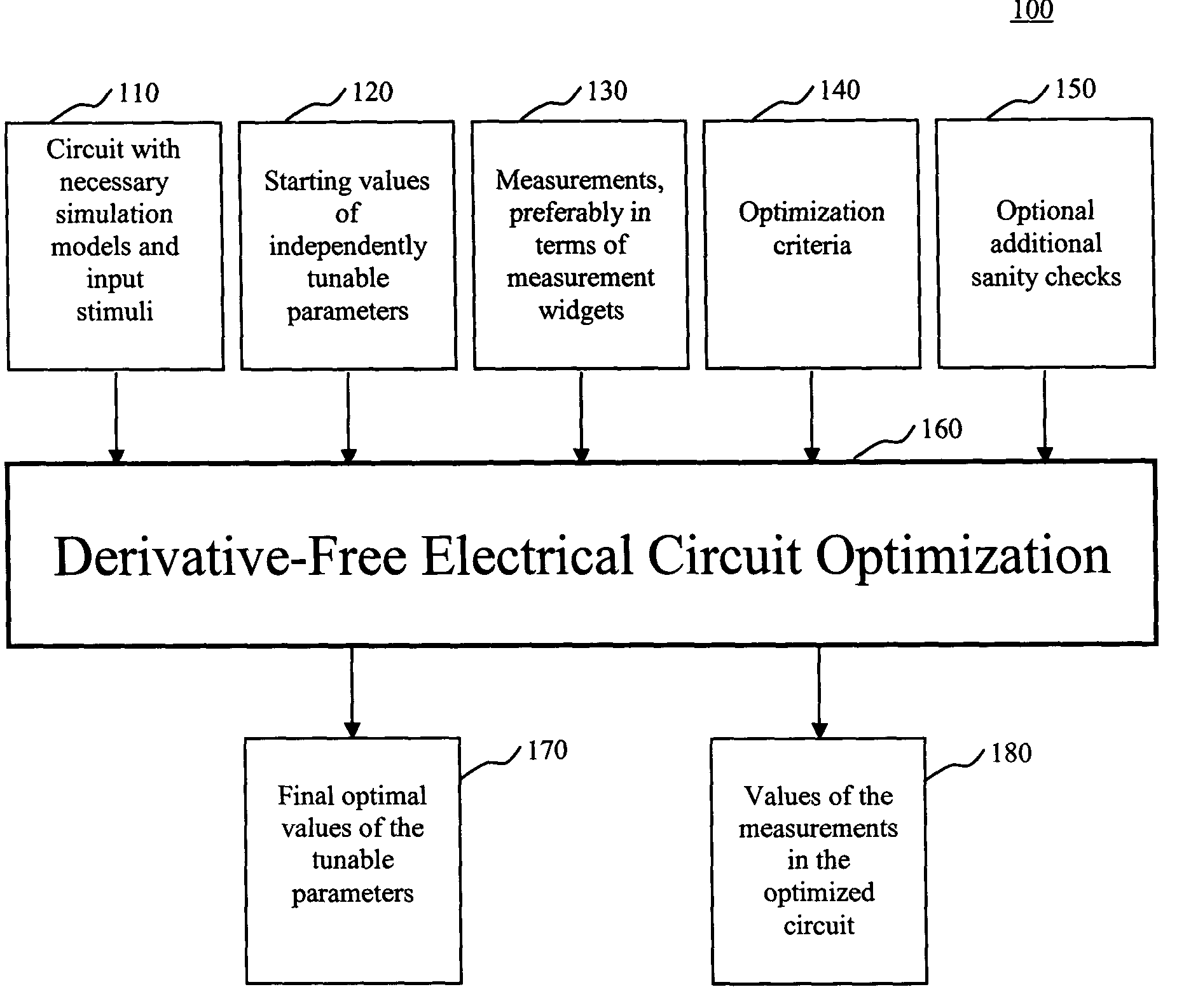
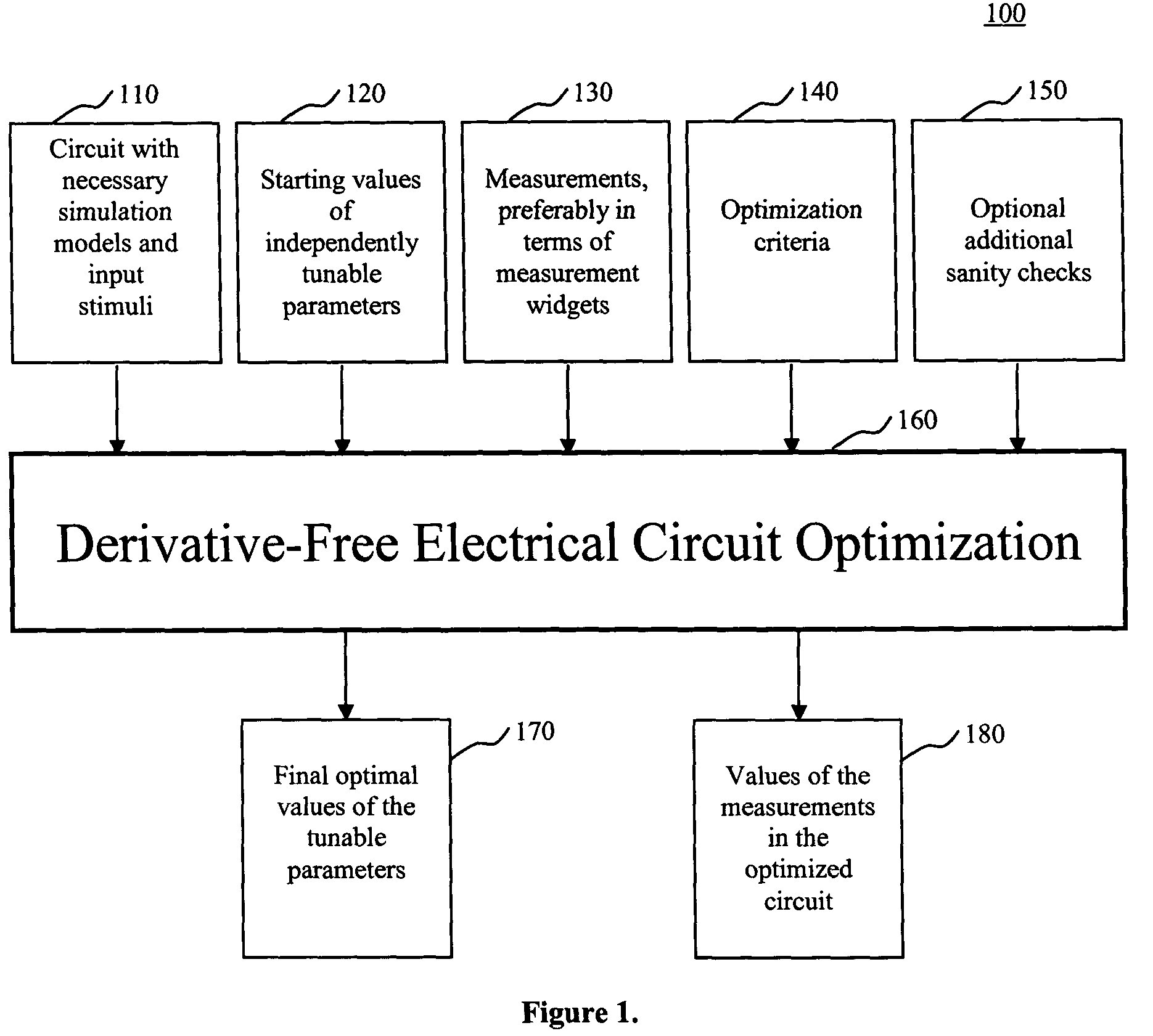
An inventive circuit optimization flow is shown in the block diagram FIG. 1, and labeled as flow 100. There are five sets of inputs to the inventive circuit optimization. The first, labeled box 110, is the circuit description together with all the information necessary to simulate the circuit such as device models and wire models. Also included in box 110 is the set of input stimuli or waveforms required to appropriately drive the circuit at its input ports. The next set of inputs, labeled box 120, is a set of starting values for the independently tunable parameters. The only requirement for the starting values is that they result in a circuit which has no electrical failures. It is to be noted that violation of one or more constraints does not constitute an electrical failure. The next set of inputs, labeled box 130, is a set of measurements. A measurement is a circuit response or circuit behavior which is determined from the simulation of the circuit. The inventive circuit optimi...


PUM


Abstract

The present invention is a system and method for optimizing electrical circuits by means of derivative-free optimization. Tunable parameters such as component values, transistor sizes or model parameters are automatically adjusted to obtain an optimal circuit. Any method of measuring the performance of the circuit, including computer simulation, can be incorporated into the optimization technique, with no derivative requirements. An arbitrary continuous optimization problem can be posed, including an objective function, equality and inequality constraints, and simple bounds on the tunable parameters. The optimization technique is efficient and guarantees that it will find a locally optimal solution from any starting point. Further, the procedure includes a method of automatically recovering from electrical failure to enable automatic and productive circuit optimization. A set of measurement widgets is provided to automatically introduce the checking required to recover from electrical failure. The automated circuit optimization leads to higher quality circuits, increases designer productivity, results in a better understanding of the tradeoffs inherent in the circuit and lifts the thinking of the circuit designer to a higher level.

Description

FIELD OF THE INVENTION This invention relates to electrical circuit design. More specifically, the invention relates to optimization of electrical circuits by tuning electrical parameters such as component values, transistor sizes and model parameters. Even more specifically, the invention relates to the optimization of electrical circuits using any method of evaluation of circuit behavior (such as a circuit simulation computer program) that does not produce derivatives. BACKGROUND OF THE INVENTION Electrical engineers spend a great deal of effort optimizing circuits. The goal of the optimization may be to minimize the delay or power of the circuit, subject to certain constraints. The optimization is carried out by adjusting or tuning electrical parameters such as component values, transistor sizes and model parameters. Traditionally, electrical engineers simulate the circuit using a circuit simulation computer program to determine the behavior and performance of the circuit. They...

Claims


Application Information

Patent Timeline
IPC IPC(8): G06F17/50
CPCG06F17/5063G06F17/505G06F30/36G06F30/327G06F30/373
Inventor WALKER, STEVEN G.VISWESWARIAH, CHANDRAMOULISCHEINBERG, KATYARESTLE, PHILLIP
Owner IBM CORP
Learn More