Scintillator panel, method of manufacturing scintillator panel, radiation detection device, and radiation detection system
- Summary
- Abstract
- Description
- Claims
- Application Information
AI Technical Summary
Benefits of technology
Problems solved by technology
Method used
Image

Examples
embodiment 1
[0069] (Embodiment 1)
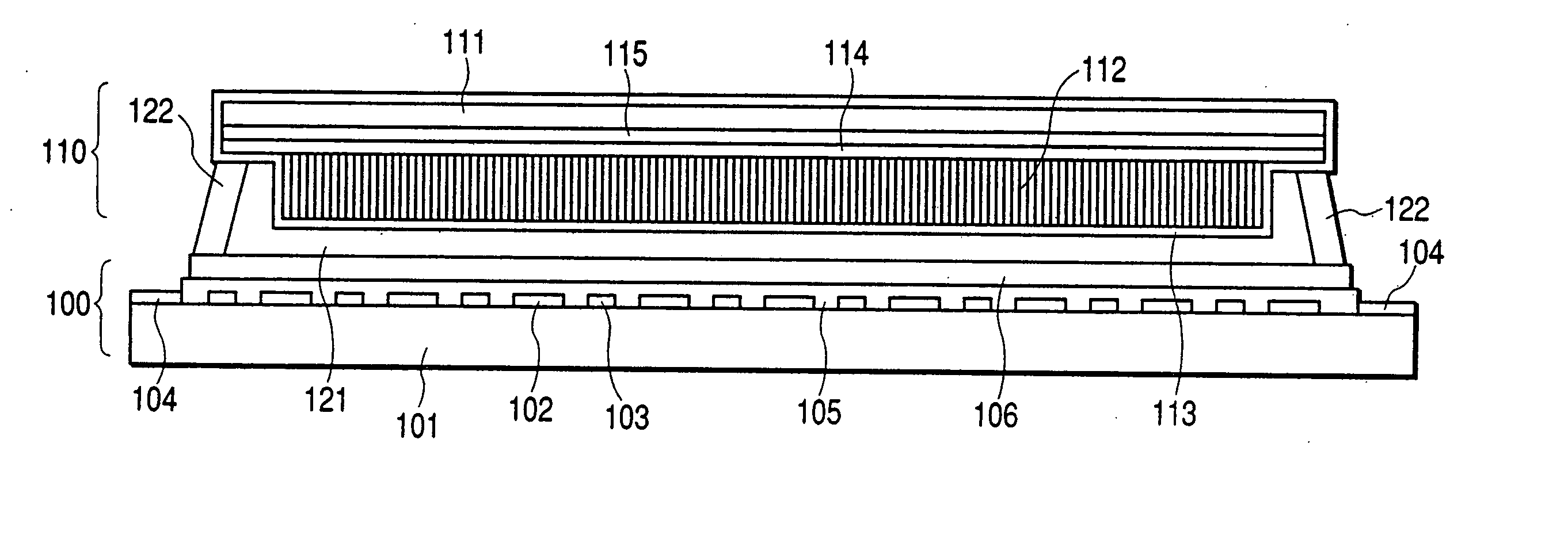
[0070]FIG. 1 is a schematic cross sectional view of a radiation detection device of this embodiment. In FIG. 1, reference numeral 110 denotes a scintillator. This scintillator includes a phosphor 112 which is used as a wavelength converter for converting radiation into light, made of alkali halide, and crystallized in a column shape, a base member 111 made of amorphous carbon or the like for supporting the phosphor 112, a reflective layer 114 made from an aluminum thin film for reflecting light converted by the phosphor 112 to a sensor panel 100 side described later, an insulating film 115 which is formed between the base member 111 and the reflective layer 114 and made of SiNx or the like, and a protective layer 113 made of an organic resin for protecting the phosphor 112 and the like from outside air. This reflective layer also serves to prevent entrance of scattering light such as outside light into a sensor.
[0071] Since strong bond is produced between silic...
embodiment 2
[0085] (Embodiment 2)
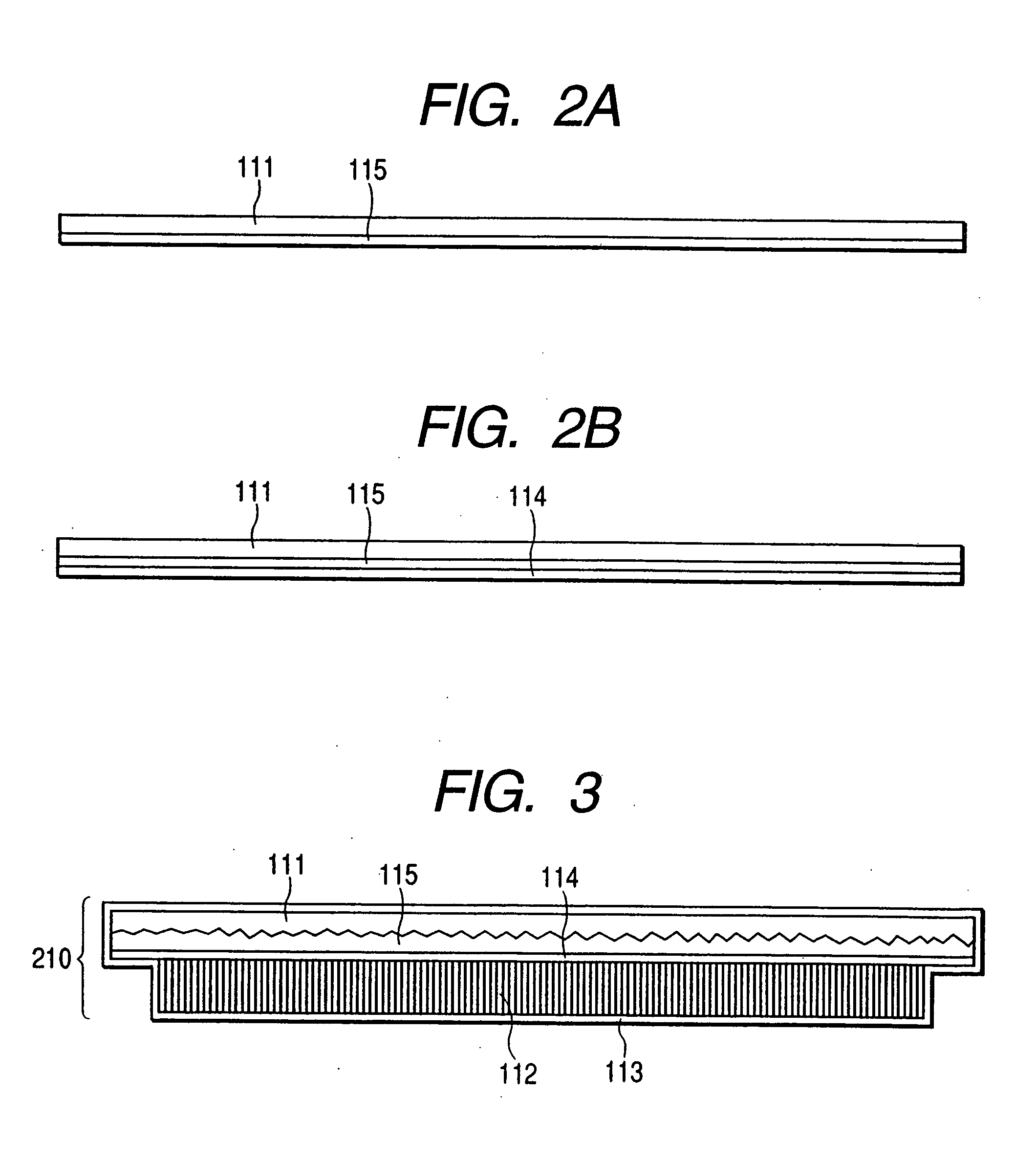
[0086]FIG. 3 is a cross sectional view of a scintillator 210 according to a radiation detection device of this embodiment. In this embodiment, polyimide is used for an insulating layer 115. Also, the surface of a base member 111 is made rough such that the adhesion to the insulating layer 115 is improved. Thus, the adhesion power due to an anchor effect is obtained between the insulating layer 115 and the base member 111. It may not be made rough in accordance with a state of the surface of the base member to be used.
[0087] Note that the same reference symbols are used for the same portions as FIG. 1 in FIG. 3. Also, with respect to a sensor panel 100, the same one as FIG. 1 is preferably used.
[0088] The base member 111 is not flat surface. However, when the insulating layer 115 is provided to make the surface of the insulating film flat, a reflective layer 114 can be formed to be flat and the surface of the reflective layer 114 can be made to obtain mirror re...
embodiment 3
[0095] (Embodiment 3)
[0096]FIG. 5 is a cross sectional view of a scintillator 310 according to a radiation detection device of Embodiment 3 of the present invention. In this embodiment, a divinylsiloxanebisbenzobutene based resin (hereinafter referred to as a “BCB”) is used for an insulating layer 115. Also, a second insulating layer 116 made of SiNx or the like is provided between the insulating layer 115 and a reflective layer 114. Note that the same reference symbols are used for the same portions as FIG. 3 in FIG. 5. Also, with respect to a sensor panel 100, the same one as FIG. 1 is used.
[0097] With respect to the scintillator 310 shown in FIG. 5, as in the case of the scintillator shown in FIG. 3, the surface of a base member 111 is made rough to improve the adhesion to the insulating layer 115 and the surface of the insulating layer 115 is also flat. The film thickness of the insulating layer 115 is preferably determined as in the case of FIG. 3 and a preferable thickness is...
PUM
 Abstract
Description
Claims
Application Information
 - R&D Engineer
- R&D Manager
- IP Professional
- Industry Leading Data Capabilities
- Powerful AI technology
- Patent DNA Extraction
Browse by: Latest US Patents, China's latest patents, Technical Efficacy Thesaurus, Application Domain, Technology Topic.
© 2024 PatSnap. All rights reserved.Legal|Privacy policy|Modern Slavery Act Transparency Statement|Sitemap