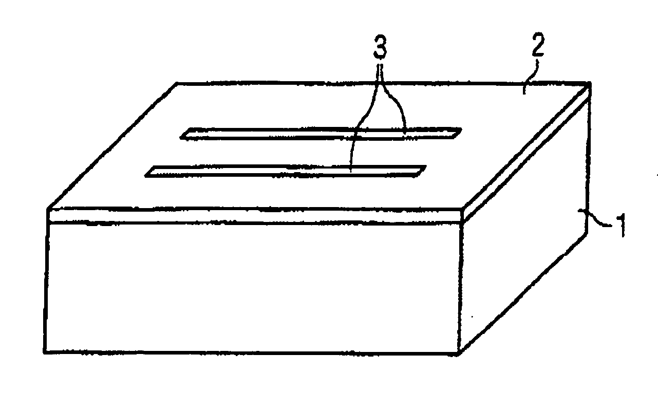
Semiconductor chip with FIB protection
a technology of semiconductor chips and fibs, which is applied in the direction of semiconductor/solid-state device details, electrical equipment, credit or payment cards, etc., can solve the problems of unsecured semiconductor chips used in chip cards, which are susceptible to attacks for decoding memory contents or chip functions,
- Summary
- Abstract
- Description
- Claims
- Application Information
AI Technical Summary
Problems solved by technology
Method used
Image

Examples
example
[0023] In a specific configuration of the semiconductor chip, a 500 nm thick layer of a polyaromatic dielectric was applied and cured. In this dielectric, conducting layers lying next to one another with a width of 250 nm, a spacing of 200 nm and a length of 1 mm were etched with a curing mask and a reactive ion plasma. After the deposition of a starter coat of titanium nitride (TiN) and copper, electrolytic thickening was carried out and excess copper was removed by means of CMP (chemical mechanical polishing).
[0024] Electrical measurements on this semiconductor chip showed no significant ohmic conduction between the conductive tracks. The dielectric was exposed in an FIB device to gallium ions with an acceleration voltage of 50 keV. A reduction in the resistance between the conductive tracks was then observed. An acceleration voltage of as little as 30 keV would have been sufficient.
PUM
 Abstract
Description
Claims
Application Information
 - R&D
- Intellectual Property
- Life Sciences
- Materials
- Tech Scout
- Unparalleled Data Quality
- Higher Quality Content
- 60% Fewer Hallucinations
Browse by: Latest US Patents, China's latest patents, Technical Efficacy Thesaurus, Application Domain, Technology Topic, Popular Technical Reports.
© 2025 PatSnap. All rights reserved.Legal|Privacy policy|Modern Slavery Act Transparency Statement|Sitemap|About US| Contact US: help@patsnap.com