Substrate for liquid crystal display device, manufacturing method of the same, and liquid crystal display device having the same
a technology of liquid crystal display device and substrate, which is applied in non-linear optics, instruments, optics, etc., can solve the problems of high degree of undulation of substrate surface, difficult to obtain uniform cell thickness by spraying spacers, and difficult to obtain uniform cell thickness distribution. , to achieve the effect of good display characteristics and high luminan
- Summary
- Abstract
- Description
- Claims
- Application Information
AI Technical Summary
Benefits of technology
Problems solved by technology
Method used
Image

Examples
embodiment 1-1
[0057]
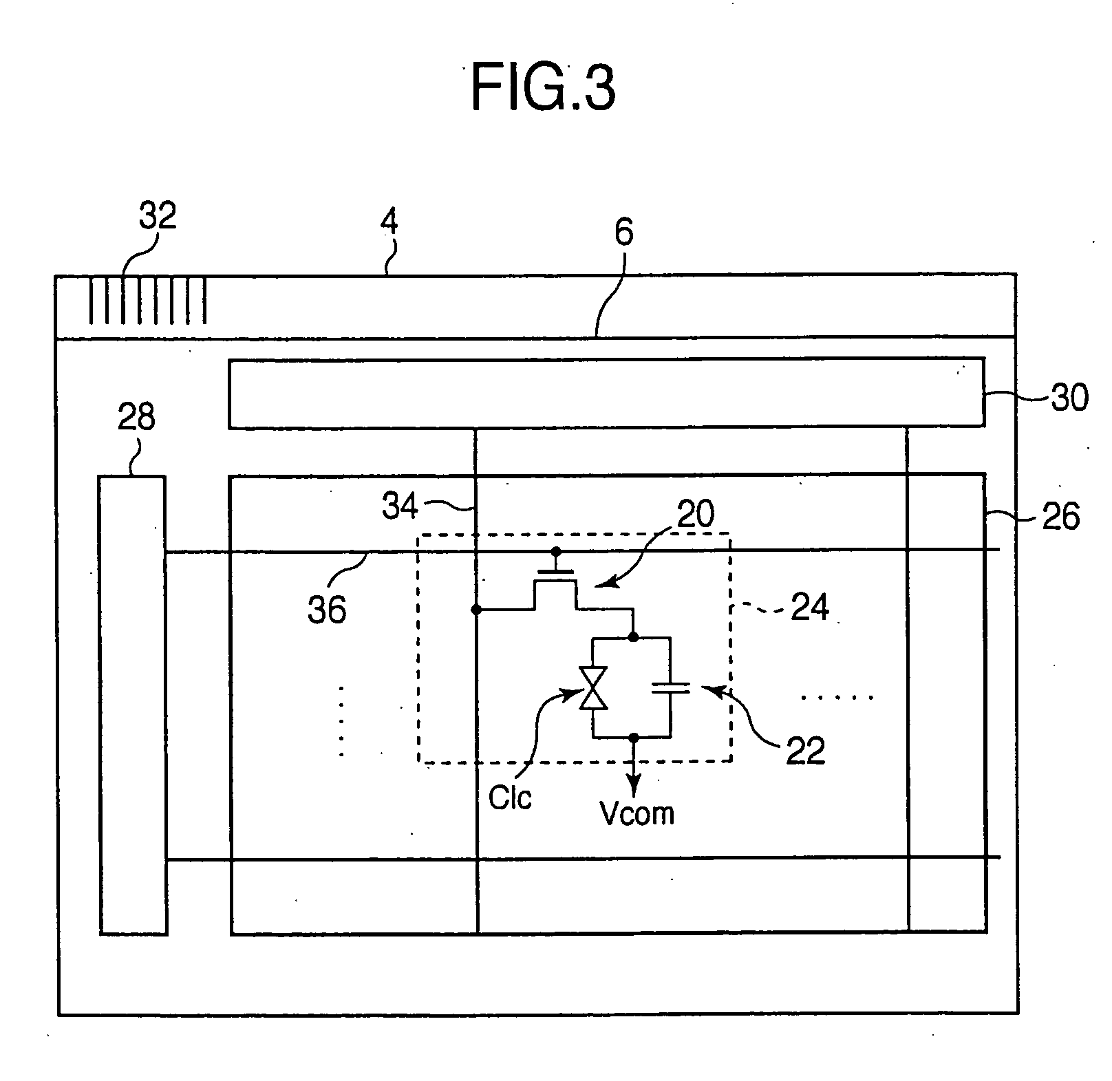
[0058] A substrate for a liquid crystal display device, manufacturing method of the substrate, and a liquid crystal display device having the substrate according to this embodiment will be described below with reference to FIGS. 3 to 12. FIG. 3 shows the entire configuration of the liquid crystal display device according to this embodiment. A display area 26 in which a number of pixel regions 24 each having a TFT 20, a storage capacitor 22 and a pixel electrode (not shown in FIG. 3) that is a transparent conductive film made of, for example, indium tin oxide (ITO) are arranged in a matrix form is defined on an array substrate 4. In FIG. 3, an equivalent circuit corresponding to one pixel of the liquid crystal display device is shown in the pixel region 24. A gate bus line driving circuit 28 is disposed on the left of the display area 26 and a drain bus line driving circuit 30 is disposed above the display area 26 (see FIG. 3). Input terminals 32 for receiving a dot clock signa...
embodiment 1-2
[0070]
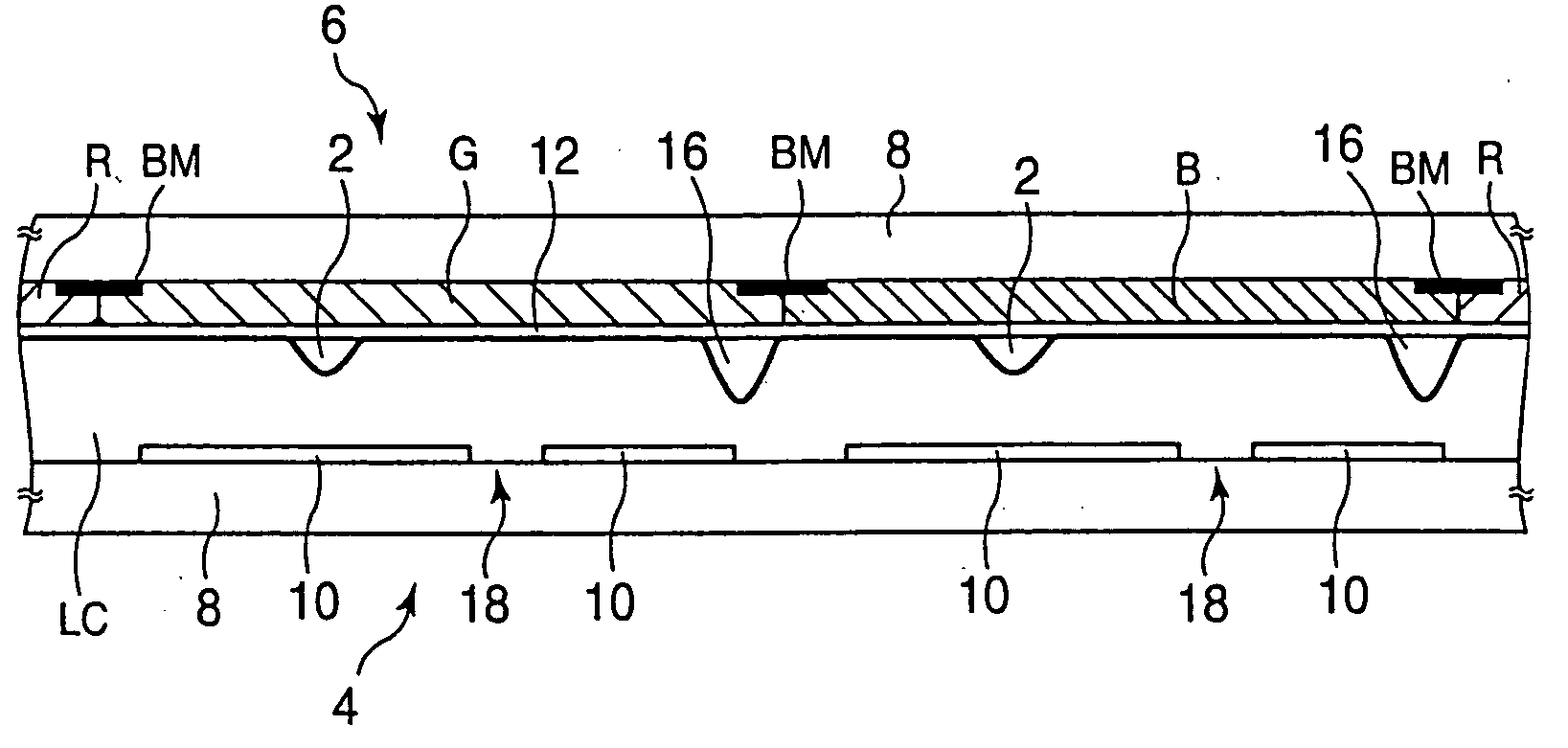
[0071] A substrate for a liquid crystal display device, manufacturing method of the substrate, and a liquid crystal display device having the substrate according to this embodiment will be described below with reference to FIGS. 13 to 18. First, the configuration of the substrate for a liquid crystal display device and the configuration of the liquid crystal display device using the substrate according to this embodiment will be outlined with reference to FIGS. 13 and 14. The entire configuration of the liquid crystal display device is the same as in Embodiment 1-1 (see FIG. 3) and hence will not be described. FIG. 13 is a plan view showing the configuration of a CF substrate 6 as a substrate for a liquid crystal display device according to this embodiment and, more specifically, shows three pixels of R, G, and B on the CF substrate 6. FIG. 14 is a sectional view of the substrate for a liquid crystal display device taken along line E-E in FIG. 13. The components in FIGS. 13 an...
embodiment 2-2
[0113]
[0114] Also in this embodiment, how resin spacers 54 are formed on a CF substrate 56 will be described with reference to FIGS. 32 to 34. A BM, color filters R, G, and B, and a common electrode 52 are formed in the same manners as in Embodiment 2-1. Informing the color filters R, G, and B, as shown in FIG. 29 (used for the description of Embodiment 2-1), resin spacer 54 forming surfaces are formed by laminating three color filter forming layers one on another in BM regions, thereby forming resin spacers 54 for regulating the cell thickness. Thus, the resin spacer forming surfaces are made higher than the surfaces of the other regions.
[0115] Then, a novolak resin type, positive, photosensitive photoresist is applied to a glass substrate 50 at a thickness of 3 μm. As shown in FIG. 32, not only a plurality of resin spacers 54 (only one resin spacer 54 is shown in FIG. 32) and a plurality of dummy patterns 64 but also dummy test patterns 66 are formed through exposure by a proximi...
PUM
 Abstract
Description
Claims
Application Information
 - Generate Ideas
- Intellectual Property
- Life Sciences
- Materials
- Tech Scout
- Unparalleled Data Quality
- Higher Quality Content
- 60% Fewer Hallucinations
Browse by: Latest US Patents, China's latest patents, Technical Efficacy Thesaurus, Application Domain, Technology Topic, Popular Technical Reports.
© 2025 PatSnap. All rights reserved.Legal|Privacy policy|Modern Slavery Act Transparency Statement|Sitemap|About US| Contact US: help@patsnap.com