Method for generating constrained component placement for integrated circuits and packages

Inactive Publication Date: 2005-02-03
CADENCE DESIGN SYST INC
View PDF10 Cites 11 Cited by
  • Summary
  • Abstract
  • Description
  • Claims
  • Application Information

AI Technical Summary

Benefits of technology

[0042] Step (c) can include, for components tagged for placement on the same side of the global symmetry line, placing a component associated with a leaf positioned lower in the tree structure closer to the global symmetry line than a component asso

Problems solved by technology

Integrated circuit and electronic board/package design is subject to complex geometric and electrical rules governing the allowed placement of components.
Component placements which fail to abide by these rules may occupy too much area to be economically manufactured, achieve levels of desired performance far below those specified at the outset of the design process, or even fail to perform their desired function correctly.
However, for placements intended to create layouts that incorporate non-digital components, for example, analog components, mixtures of analog and digital components (called “mixed-signal” designs), radio-frequency components (“RF”) and microwave-frequency components, among others, additional geometric constraints are often imposed.
These prior art methods, however, do not work when the presence of arbitrary combinations

Method used


Image

  • Method for generating constrained component placement for integrated circuits and packages
  • Method for generating constrained component placement for integrated circuits and packages
  • Method for generating constrained component placement for integrated circuits and packages

Examples


Embodiment Construction

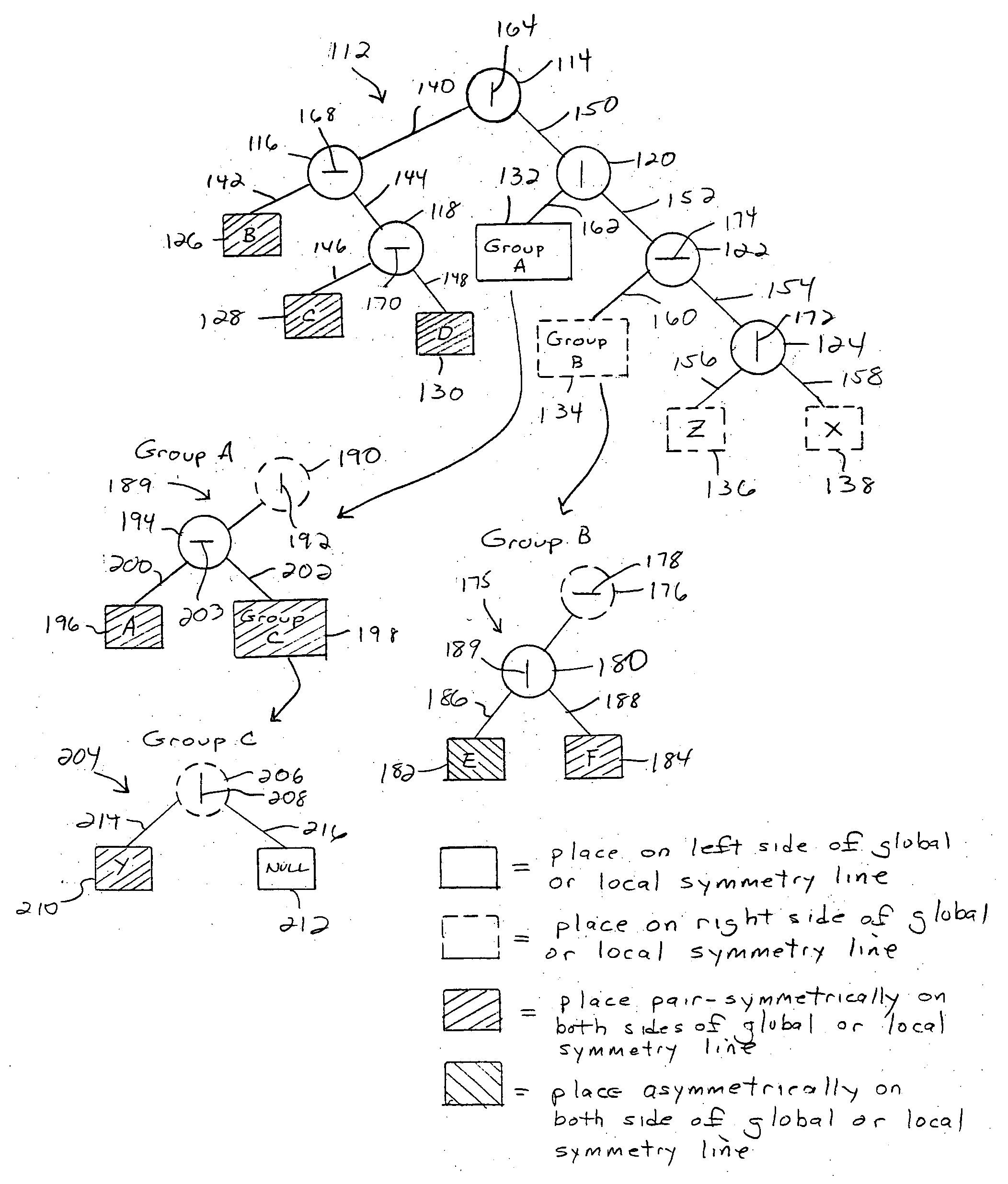
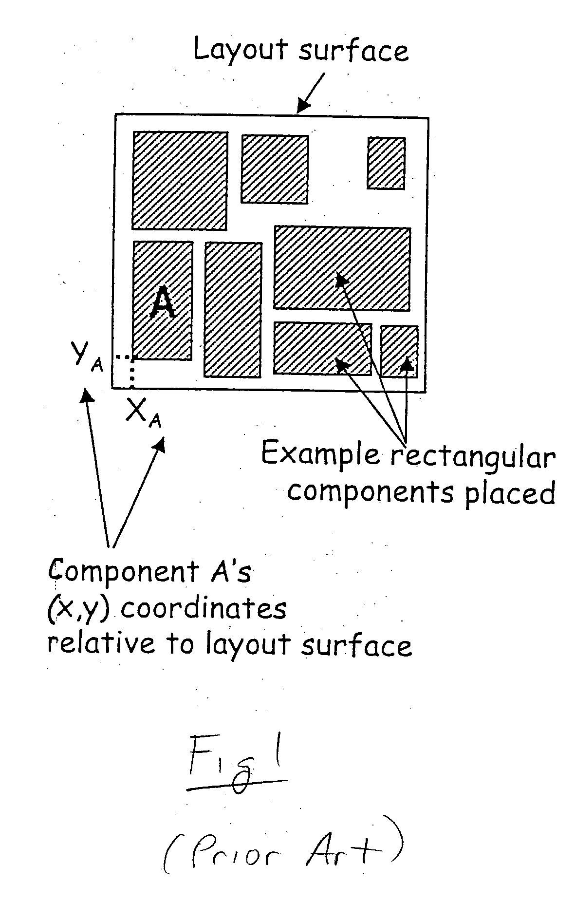
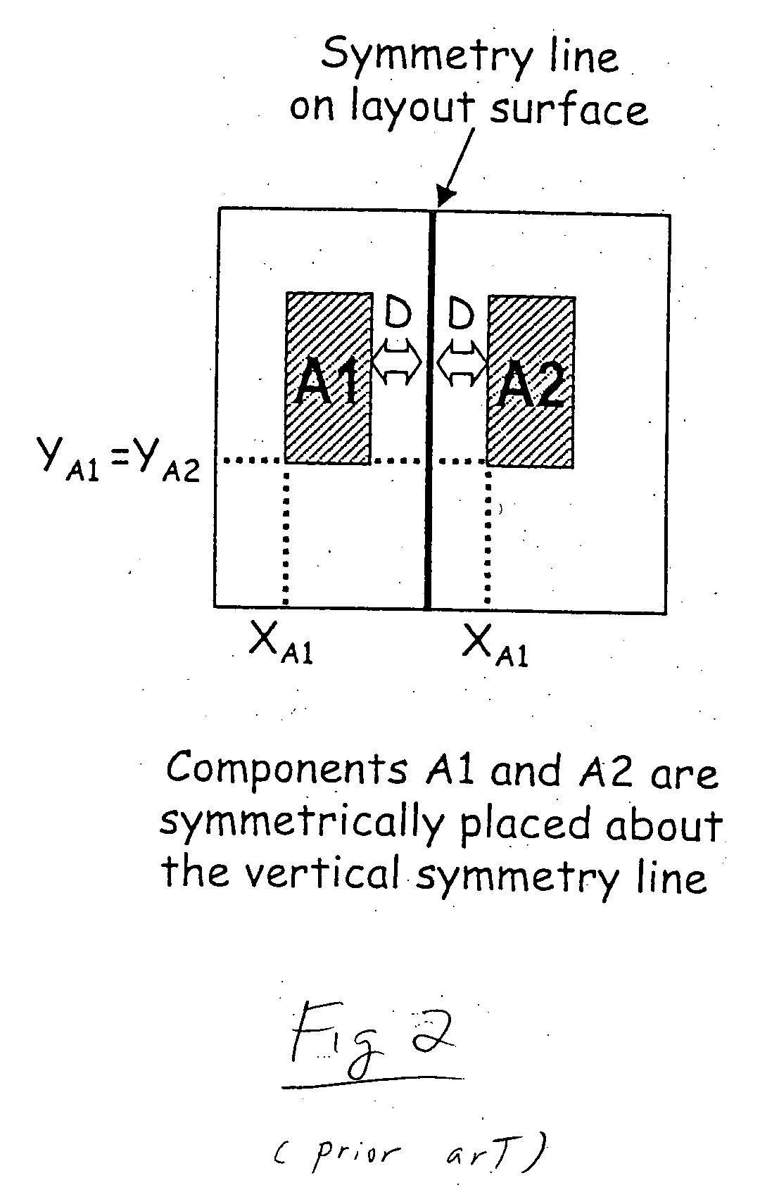
[0116] The present invention will be described with reference to the accompanying figures where like nomenclature refer to like elements. Moreover, the terms left, right, top, bottom, horizontal, vertical and the like are used with reference to the accompanying figures and are not to be construed as limiting the invention.

[0117] The present invention is embodied in computer readable program code that executes on a processor of a stand-alone or networked computer or workstation that includes a processor, computer storage, an input / output system, a media drive, such as a disk drive, CD ROM drive, etc., and a computer-useable storage medium capable of storing the computer software that embodies the present invention. Under the control of the computer readable program code, the processor is capable of configuring and operating the computer system in a manner to implement the present invention. Computer systems of the type described above are well known in the art and have not been desc...


PUM


Abstract

A method for determining component placement in a circuit includes forming a tree structure that defines the placement of each of a plurality of components associated with the tree structure on a first side, a second side or on both sides of a symmetry line, with at least one component tagged for symmetric placement on both sides of a symmetry line; performing at least one search of the tree structure to determine an initial placement of a subset of the components; and performing another search of the tree structure to determine a final placement of the subset of components whereupon at least a part of each component tagged for symmetric placement is positioned on each side of the symmetry line. The method can be embodied as instructions stored on a computer readable medium which, when executed by a processor, cause the processor to implement the method.

Description

CROSS REFERENCE TO RELATED APPLICATIONS [0001] This application claims priority from U.S. Provisional Patent Application No. 60 / 415,625, filed Oct. 2, 2002.BACKGROUND OF THE INVENTION [0002] 1. Field of the Invention [0003] The present invention relates to circuit design and, more particularly, to component placement in a circuit design. [0004] 2. Description of the Prior Art [0005] Integrated circuit and electronic board / package design is subject to complex geometric and electrical rules governing the allowed placement of components. Component placements which fail to abide by these rules may occupy too much area to be economically manufactured, achieve levels of desired performance far below those specified at the outset of the design process, or even fail to perform their desired function correctly. [0006] A “component” may be an individual electronic device (for example, a transistor) or a set of pre-placed devices to be treated as a single, atomic placeable object. A “group” ma...

Claims


Application Information

Patent Timeline
IPC IPC(8): G06F17/50
CPCG06F17/5072G06F30/392
Inventor FALLON, ELIASRUTENBAR, ROB A.
Owner CADENCE DESIGN SYST INC
Why Eureka
Try Eureka