Driving method of light emitting device and light emitting device

a technology of light emitting devices and driving methods, which is applied in the direction of identification means, instruments, semiconductor devices, etc., to achieve the effect of suppressing luminance decay and variations in luminance of light emitting elements, and maintaining relatively constant drain curren

Inactive Publication Date: 2005-02-10
SEMICON ENERGY LAB CO LTD
View PDF49 Cites 55 Cited by
  • Summary
  • Abstract
  • Description
  • Claims
  • Application Information

AI Technical Summary

Benefits of technology

[0031] According to the aforementioned configuration of the invention, an N-type driving TFT can operate in a saturation region and an image can be displayed with a desired gray scale level in accordance with a video signal. Further, since the driving TFT operates in a saturation region, a drain current does not vary depending on a drain voltage Vds and is determined only by a gate voltage Vgs. Therefore, the drain current can be maintained relatively constant even when the Vds is lowered without increasing the Vel in accordance with the degradation of a light emitting element. Thus, it is possible to suppress luminance decay and variations in luminance of the light emitting element due to the degradation of an electro luminescent material.

Problems solved by technology

Explained hereinafter is a problem in using in a pixel a TFT formed of an amorphous semiconductor or a semi-amorphous semiconductor and operating a transistor for supplying a current to a light emitting element in a saturation region.

Method used


Image

  • Driving method of light emitting device and light emitting device
  • Driving method of light emitting device and light emitting device
  • Driving method of light emitting device and light emitting device

Examples


embodiment 1

[0069] Embodiment 1

[0070] Described in this embodiment is an example of the light emitting device, in which the power supply lines are arranged parallel to the scan lines in the pixel portion shown in FIG. 2 and one scan line driver circuit controls both the scan lines and the power supply lines.

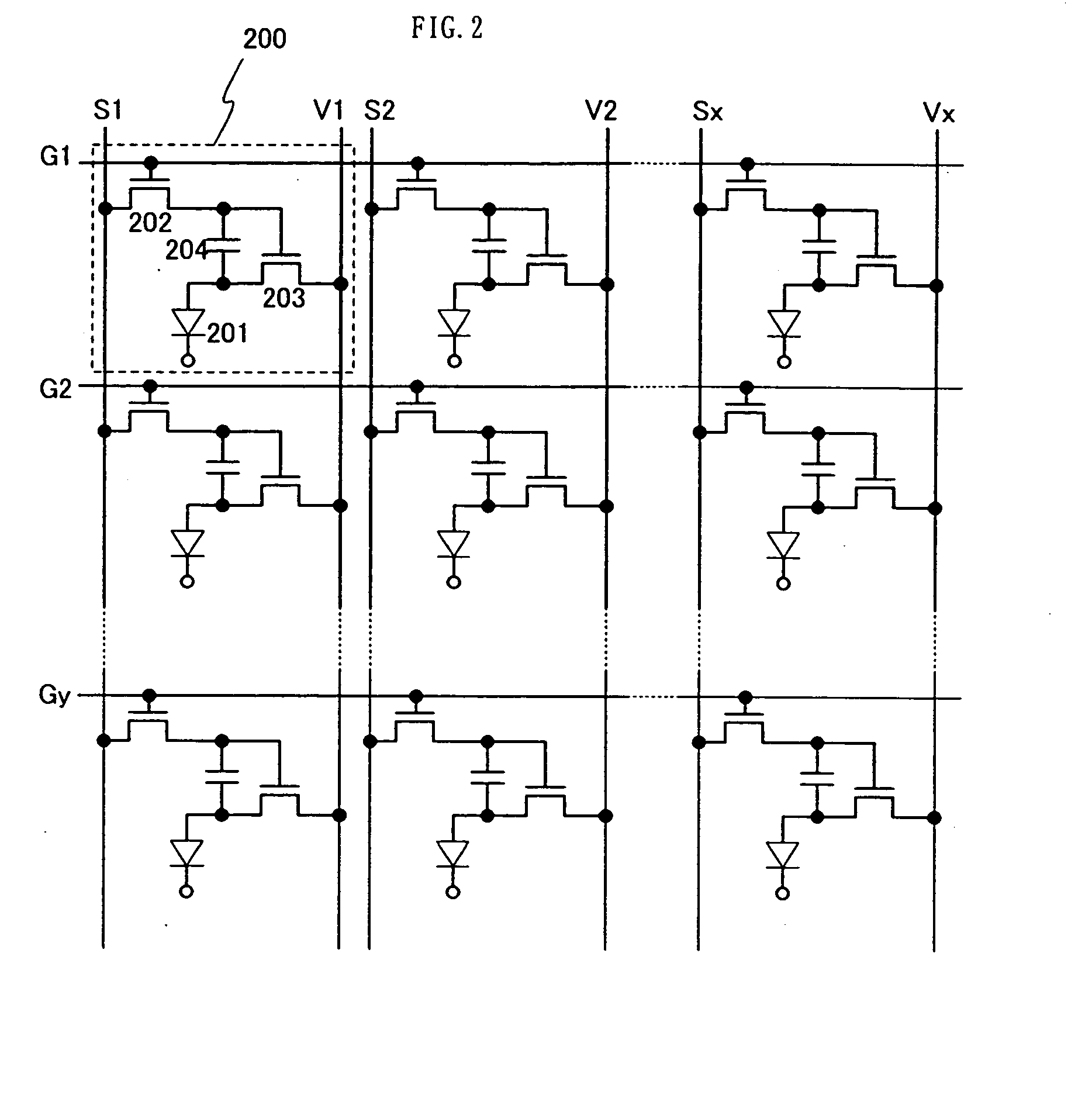
[0071]FIG. 4 shows a configuration of a pixel portion 401 in a light emitting device according to this embodiment. In FIG. 4, a pixel 400 comprises a light emitting element 405, a switching TFT 402, a driving TFT 403, and a capacitor 404 as the pixel portion shown in FIG. 2. The connection of each element is the same as that of the pixel 200 shown in FIG. 2. However, the power supply lines V1 to Vy are arranged parallel to the scan lines G1 to Gy in this embodiment.

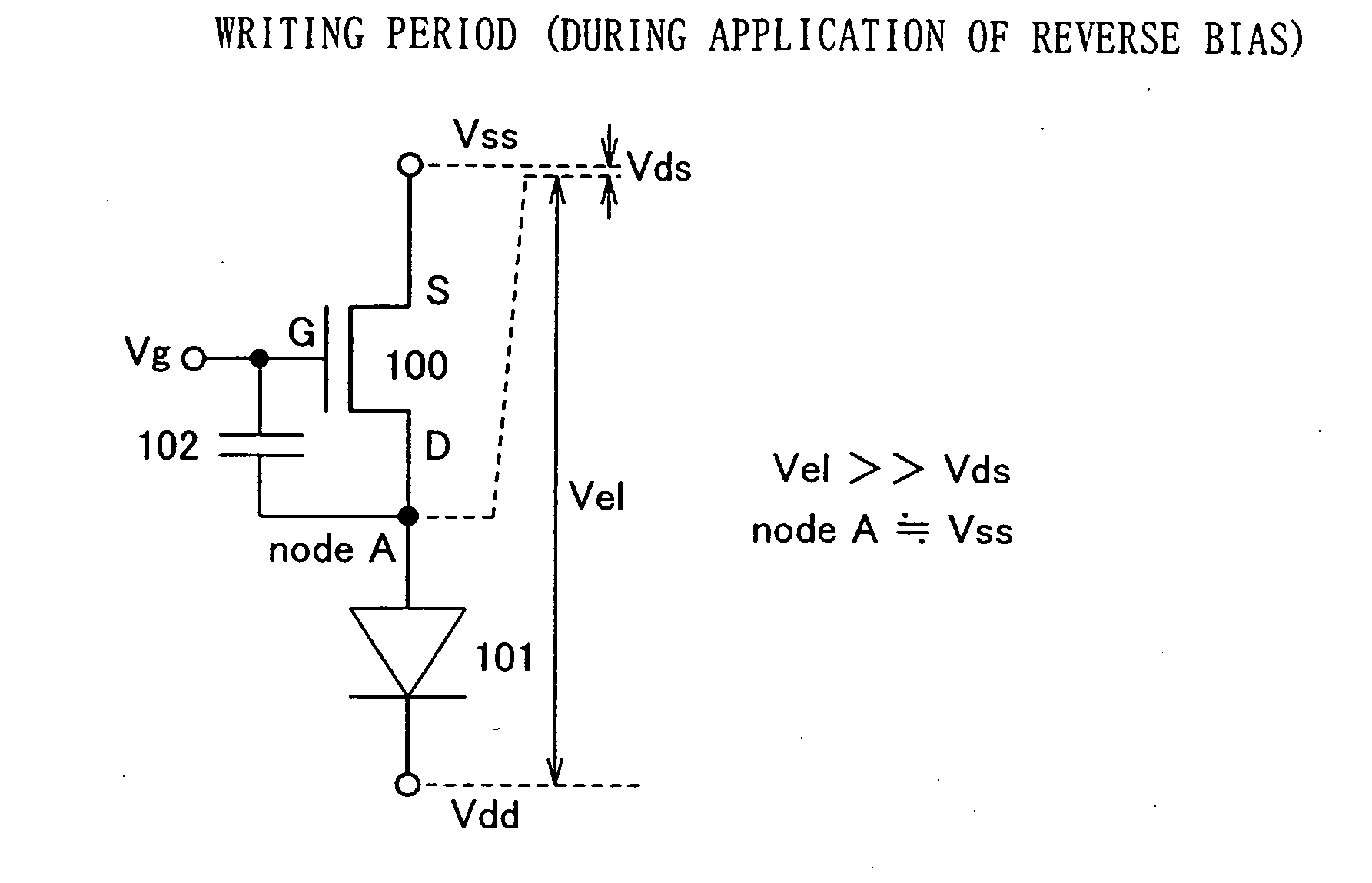
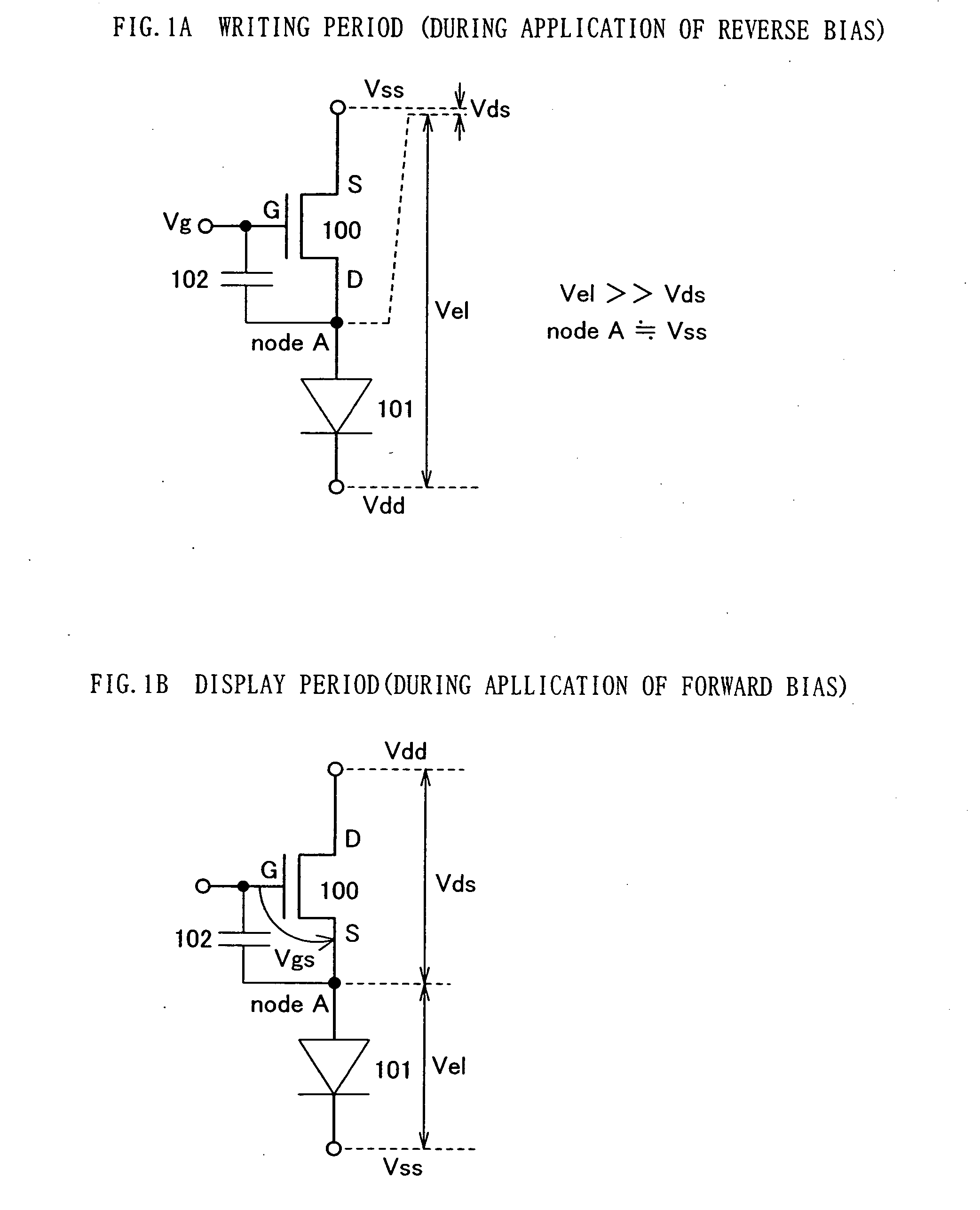
[0072] A driving method of the pixel portion shown in FIG. 4 is described next. The driving method of the invention can be divided into a writing period Ta, a reverse bias period Tr and a display period Td. FIG. 20A shows an exa...

embodiment 2

[0087] Embodiment 2

[0088] Described in this embodiment is a pixel configuration of a light emitting device capable of adopting the driving method of the invention.

[0089] A pixel shown in FIG. 6A comprises a light emitting element 601, a switching TFT 602, a driving TFT 603, an erasing TFT 604 for forcibly stopping light emission of the light emitting element 601, and a capacitor 605. A gate of the switching TFT 602 is connected to a first scan line Gaj (j=1 to y), either a source or a drain thereof is connected to a signal line Si (i=1 to x), and the other thereof is connected to a gate of the driving TFT 603. Either a source or a drain of the driving TFT 603 is connected to a power supply line Vj (j=1 to y) and the other thereof is connected to an anode of a light emitting element 601. A gate of the erasing TFT 604 is connected to a second scan line Gbj (j=1 to y), either a source or a drain thereof is connected to the gate of the driving TFT 603, and the other thereof is connecte...

embodiment 3

[0102] Embodiment 3

[0103] In the case of using TFTs formed of a semi-amorphous semiconductor (semi-amorphous TFTs) for the light emitting device of the invention, a driver circuit can be integrally formed on the same substrate as a pixel portion. Meanwhile, in the case of using TFTs formed of an amorphous semiconductor (amorphous TFTs), a driver circuit formed on another substrate may be mounted on the same substrate as a pixel portion.

[0104]FIG. 8A shows an example of an element substrate in which a pixel portion 6012 is formed on a substrate 6011 and connected to a signal line driver circuit 6013 formed separately. The pixel portion 6012 and scan line driver circuits 6014 are formed by using semi-amorphous TFTs. The signal line driver circuit 6013 is formed of transistors which exhibit a higher mobility than the semi-amorphous TFTs. As a result, it is possible to stabilize the operation of the signal line driver circuit which is required to operate at a higher frequency than the ...


PUM


Abstract

A driving method of a light emitting device, in which when an N-type driving TFT is connected to an anode of a light emitting element or a P-type driving TFT is connected to a cathode thereof, the driving TFT operates in a saturation region and an image can be displayed with a desired gray scale level depending on a video signal. In addition, a light emitting device adopting the driving method is provided. According to the invention, when a potential having image data is supplied to a gate of a driving TFT depending on a video signal, a reverse bias voltage is applied to the driving TFT and a light emitting element which are connected in series with each other. Meanwhile, when a pixel displays an image depending on the video signal, a forward bias voltage is applied to the driving TFT and the light emitting element.

Description

BACKGROUND OF THE INVENTION [0001] 1. Field of the Invention [0002] The invention relates to a driving method of a light emitting device comprising a plurality of pixels each of which includes a light emitting element and a means for supplying a current to the light emitting element. The invention further relates to a light emitting device. [0003] 2. Description of the Related Art [0004] Emitting light by itself, a light emitting element has a high visibility. Further, since it requires no backlight, a display device using the light emitting element can be easily reduced in thickness and the viewing angle thereof is not restricted. Therefore, the light emitting device using a light emitting element, which attracts attention as an alternative display device to a CRT or an LCD, has been developed for practical use. The light emitting device can be classified into a passive matrix device and an active matrix device. In the active matrix device, a current supply to a light emitting elem...

Claims


Application Information

Patent Timeline
Patent Type & Authority Applications(United States)
IPC IPC(8): G09F9/30G09G3/20G09G3/30
CPCG09G3/2022G09G3/3233G09G3/3258G09G3/3291G09G2300/0842G09G2300/0866H01L2924/0002G09G2310/0256G09G2310/0262H01L2924/00H10K59/131H10K59/1213H10K59/1216H01L29/78669H01L29/78678G09G3/32G09G2300/0426G09G2310/08G09G2320/0233G09G2320/043
Inventor MIYAGAWA, KEISUKE
Owner SEMICON ENERGY LAB CO LTD
Why Eureka
Try Eureka