Method for correcting pixel defect in image sensing element, and image sensing apparatus using the same

a technology of image sensing element and image sensing apparatus, which is applied in the field of image sensing apparatus, can solve the problems of degrading image quality, high cost, and high power consumption, and achieve the effect of high precision

Inactive Publication Date: 2005-02-10
CANON KK
View PDF4 Cites 77 Cited by
  • Summary
  • Abstract
  • Description
  • Claims
  • Application Information

AI Technical Summary

Benefits of technology

[0008] The present invention has been made in consideration of the above situation, and has as its object to provide an image sensing apparatus and image sensing method capable of eliminating a nonvolatile memory for storing position information of a defective pixel, and detecting a defective pixel at high precision even while sensing a complicated object.

Problems solved by technology

Such defective pixel appears as isolated point noise in an image sensed by the solid-state image sensing element, degrading the image quality.
However, this method requires a nonvolatile memory for storing pieces of position information corresponding to the number of assumed defective pixels.
This results in high cost and high power consumption.
However, if a defective pixel is detected while an image such as a natural image (image with a complicated brightness difference or color saturation difference) is sensed, the defective pixel detection precision decreases, and the image quality degrades due to correction based on erroneous detection.

Method used


Image

  • Method for correcting pixel defect in image sensing element, and image sensing apparatus using the same
  • Method for correcting pixel defect in image sensing element, and image sensing apparatus using the same
  • Method for correcting pixel defect in image sensing element, and image sensing apparatus using the same

Examples


first embodiment

[0024] (First Embodiment)

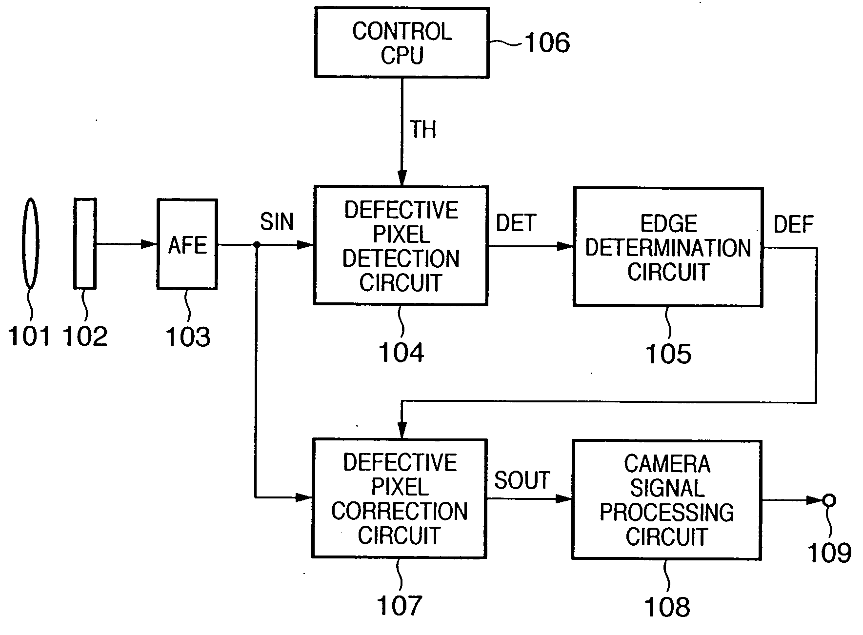
[0025]FIG. 1 is a block diagram showing the schematic arrangement of a single-CCD image sensing apparatus according to the first embodiment of the present invention. In FIG. 1, incident light traveling from an object to be sensed is formed on the image sensing plane of an image sensing element 102 via an imaging optical system (image sensing lens or the like) 101. The pixels of the image sensing element 102 are covered with a color filter for color image sensing. The image sensing element 102 is, e.g., a CCD, and the pixels of the image sensing element 102 perform photoelectric conversion in accordance with the object brightness. In the first embodiment, the color filter is prepared by periodically arraying color filters of three colors R, G, and B (Red, Green, and Blue), as shown in FIG. 3. The color filter array is not limited to this, and various arrays with combinations of various colors such as a combination of only complementary colors and a combinatio...

second embodiment

[0042] (Second Embodiment)

[0043] An image sensing apparatus according to the second embodiment that is different in an edge determination process from the image sensing apparatus according to the first embodiment will be described. FIG. 9 is a block diagram showing the schematic arrangement of an image sensing apparatus according to the second embodiment. In FIG. 9, the same reference numerals as 101, 102, 103, 104, 107., 108, and 109 in FIG. 1 denote parts having the same functions, and a description thereof will be omitted. In other words, the image sensing apparatus according to the second embodiment is different from the image sensing apparatus according to the first embodiment in that a control CPU 901 and edge determination circuit 902 are arranged.

[0044] As shown in FIG. 9, the control CPU 901 is the same as the control CPU 106 according to the first embodiment in that the control CPU 901 outputs the above-mentioned threshold TH, but different in that the control CPU 901 fur...


PUM


Abstract

An object of this invention is to provide an image sensing apparatus and image sensing method capable of eliminating a nonvolatile memory for storing position information of a defective pixel, and detecting a defective pixel at high precision even while sensing a complicated object. To achieve this object, there is provided an image sensing apparatus including a solid-state image sensing element having a plurality of pixels which output image sensing signals, a first determination device which determines whether a pixel of interest is a defective pixel candidate, by comparing the signal level of the pixel of interest subjected to defective pixel detection out of the plurality of pixels of the solid-state image sensing element, and the signal levels of a plurality of peripheral pixels around the pixel of interest, and a second determination device which, when the-first determination device determines that the pixel of interest is the defective pixel candidate, determines whether the determination result representing that the pixel of interest is the defective pixel candidate is erroneous detection, on the basis of the determination result of the first determination device representing whether a plurality of peripheral pixels around the pixel of interest are defective pixel candidates.

Description

FIELD OF THE INVENTION [0001] The present invention relates to an image sensing apparatus having an image sensing element and, more particularly, to an image sensing apparatus and image sensing method capable of correcting a pixel defect in an image sensing element during image sensing. BACKGROUND OF THE INVENTION [0002] A conventional solid-state image sensing element such as a CCD (Charge Coupled Device) suffers a so-called defective pixel in which the sensitivity is lower than that of a nondefective pixel or a very large dark current flows. Such defective pixel appears as isolated point noise in an image sensed by the solid-state image sensing element, degrading the image quality. In order to eliminate an adverse effect on the image quality, an image sensing apparatus using the solid-state image sensing element corrects a defective pixel. [0003] As conventional defective pixel correction methods, the following two methods have generally been known. [0004] According to the first c...

Claims


Application Information

Patent Timeline
Patent Type & Authority Applications(United States)
IPC IPC(8): G06T1/00H01L27/148G06T3/40H04N1/40H04N5/232H04N5/335H04N5/367H04N5/376H04N9/64
CPCH04N5/3675G06T3/403H04N25/683
Inventor HATTORI, YUUICHIROU
Owner CANON KK
Why Eureka
Try Eureka