Method for selectively controlling damascene CD bias

Inactive Publication Date: 2005-02-10
TAIWAN SEMICON MFG CO LTD
View PDF8 Cites 23 Cited by
  • Summary
  • Abstract
  • Description
  • Claims
  • Application Information

AI Technical Summary

Benefits of technology

[0011] In a first embodiment, the method includes providing a semiconductor wafer including a first opening formed extending through a thickness of at least one dielectric insulating layer and having an uppermost inorganic BARC layer; depositing a photoresist layer over the uppermost BARC layer and patterning the photoresist layer to form an etching pattern for etching a second opening overlying and encompassing the first opening; carrying out a first plasma assisted etching process to etch through a thickness of the BARC layer including a predetermined amount of CO in a plasma etching chemistry to increase an etching resistance of the photoresist layer; and, carrying out a second plasma assisted etching process to etch through a thickness portion of the at least one dielectric insulating layer to form the second opening.

Problems solved by technology
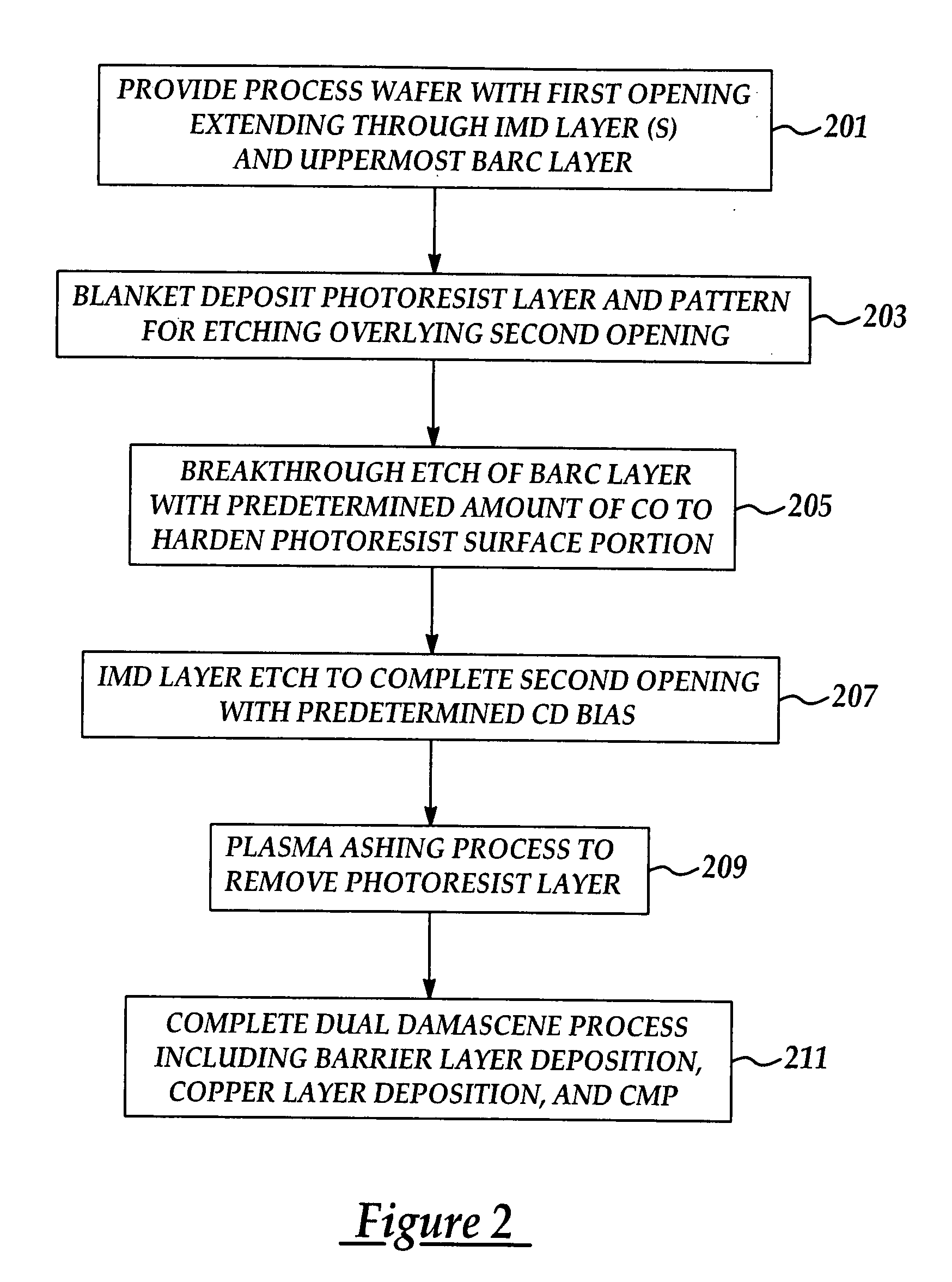
As device sizes decrease it has been increasingly difficult to provide interconnection technology that satisfies the requirements of low resistance and capacitance interconnect properties, particularly where submicron inter-layer interconnects and intra-layer interconnects have increasingly high aspect ratios (e.g., an interconnect opening depth to opening diameter (or linewidth) ratio).
One problem with achieving desired feature dimensions is the tendency of the photoresist to shrink during development and post exposure bake processes due to the loss of solvents.
Another problem with the prior art in achieving the desired control over CD bias in etched openings, for example, with linewidths and opening diameters less than about 0.25 microns, including 0.13 microns and less, is that patterned photoresists forming a patterned etch opening do not have the desired selectivity (or resistance) to an etching plasma chemistry, frequently resulting in a degree of overetching or undercutting of the sidewalls of the photoresist pattern.

Method used


Image

  • Method for selectively controlling damascene CD bias
  • Method for selectively controlling damascene CD bias
  • Method for selectively controlling damascene CD bias

Examples


Embodiment Construction

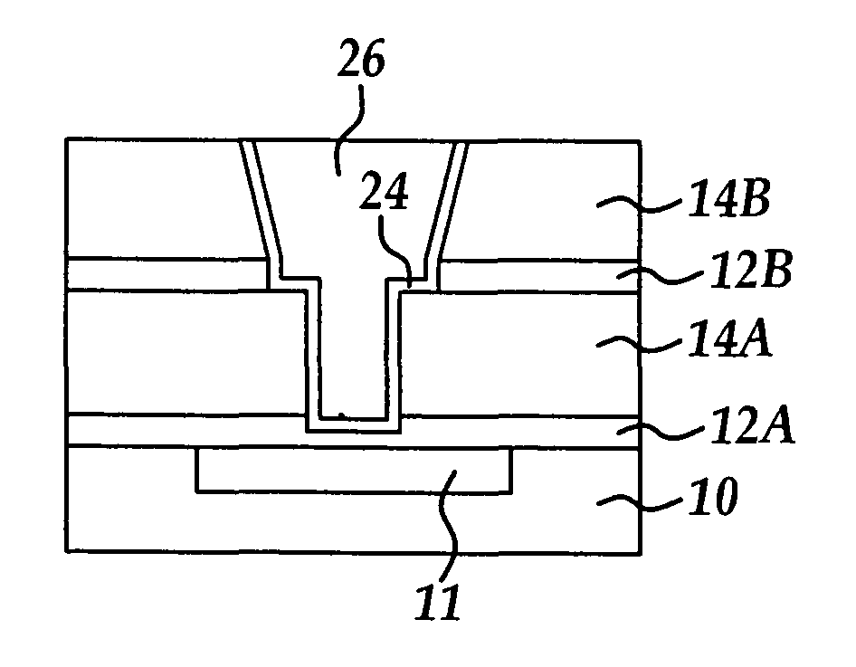
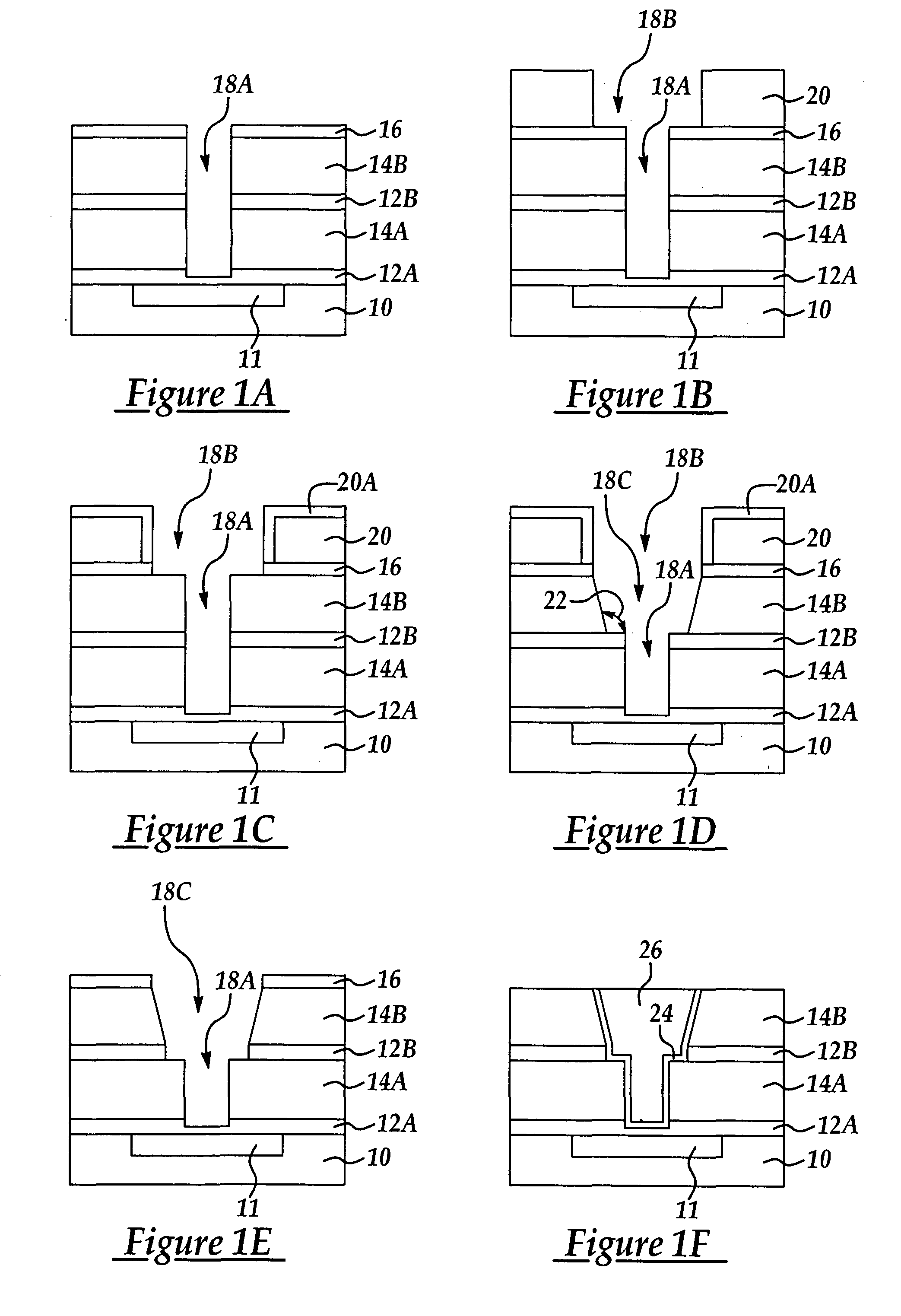
[0015] Although the method of the present invention is explained by exemplary reference the formation of a via-first method of formation of a dual damascene structure in a multi-level semiconductor device, it will be appreciated that the method of the present invention is equally applicable to plasma assisted etching of other structures including single damascenes as well as a trimming process where the opening dimension is adjusted or a sidewall profile adjusted by etching a larger sized opening to at least partially encompass an underlying opening. In general, the method is applicable to the plasma assisted etching of openings in semiconductor material layers, including dielectric insulating layers where an overlying patterned photoresist layer is present as an etching mask. It will be appreciated that the etched opening formed according to a plasma assisted etching process in the method of the present invention may be subsequently lined or filled with a variety of materials inclu...


PUM


Abstract

A method for selectively etching a semiconductor feature opening to controllably achieve a critical dimension accuracy including providing a semiconductor wafer including a first opening formed extending through a thickness of at least one dielectric insulating layer and having an uppermost inorganic BARC layer; depositing a photoresist layer over the uppermost BARC layer and patterning the photoresist layer to form an etching pattern for etching a second opening overlying and encompassing the first opening; carrying out a first plasma assisted etching process to etch through a thickness of the BARC layer including a predetermined amount of CO in a plasma etching chemistry to increase an etching resistance of the photoresist layer; and, carrying out a second plasma assisted etching process to etch through a thickness portion of the at least one dielectric insulating layer to form the second opening.

Description

FIELD OF THE INVENTION [0001] This invention generally relates to multi-layered semiconductor device micro-integrated circuitry and more particularly to a method for forming damascene and dual damascene openings in dielectric insulators with selective control over CD bias specifications in integrated micro-circuit manufacture. BACKGROUND OF THE INVENTION [0002] The escalating requirements for high density and performance associated with ultra large scale integration semiconductor wiring require increasingly sophisticated interconnection technology. As device sizes decrease it has been increasingly difficult to provide interconnection technology that satisfies the requirements of low resistance and capacitance interconnect properties, particularly where submicron inter-layer interconnects and intra-layer interconnects have increasingly high aspect ratios (e.g., an interconnect opening depth to opening diameter (or linewidth) ratio). As device sizes decrease below about 0.25 microns a...

Claims


Application Information

Patent Timeline
IPC IPC(8): H01L21/311H01L21/44H01L21/461H01L21/4763H01L21/768
CPCH01L21/31116H01L21/31138H01L21/76807H01L21/76804H01L21/31144
Inventor CHU, YIN-SHENCHEN, HUNG-MING
Owner TAIWAN SEMICON MFG CO LTD
Why Eureka
Try Eureka