Circuit designing method and a circuit designing system

a circuit design and circuit technology, applied in the field of circuit design methods and circuit design systems, can solve the problems of difficulty in answering the request to design, inability to realize the automatic generation of the description of the clock base simulation, and insufficient labor. achieve the effect of reducing the circuit scal

Inactive Publication Date: 2005-02-10
NEC ELECTRONICS CORP
View PDF16 Cites 23 Cited by
  • Summary
  • Abstract
  • Description
  • Claims
  • Application Information

AI Technical Summary

Benefits of technology

[0011] Therefore, an object of the present invention is to provide a circuit designing method and a circuit designing system which can generates the description for the clock base simulation automatically.
[0012] Another object of the present invention is to provide a circuit designing method and a circuit designing system which can genera...

Problems solved by technology

It needs labor and moreover is difficult to answer the request to design at the short time.
Es...

Method used


Image

  • Circuit designing method and a circuit designing system
  • Circuit designing method and a circuit designing system
  • Circuit designing method and a circuit designing system

Examples


Embodiment Construction

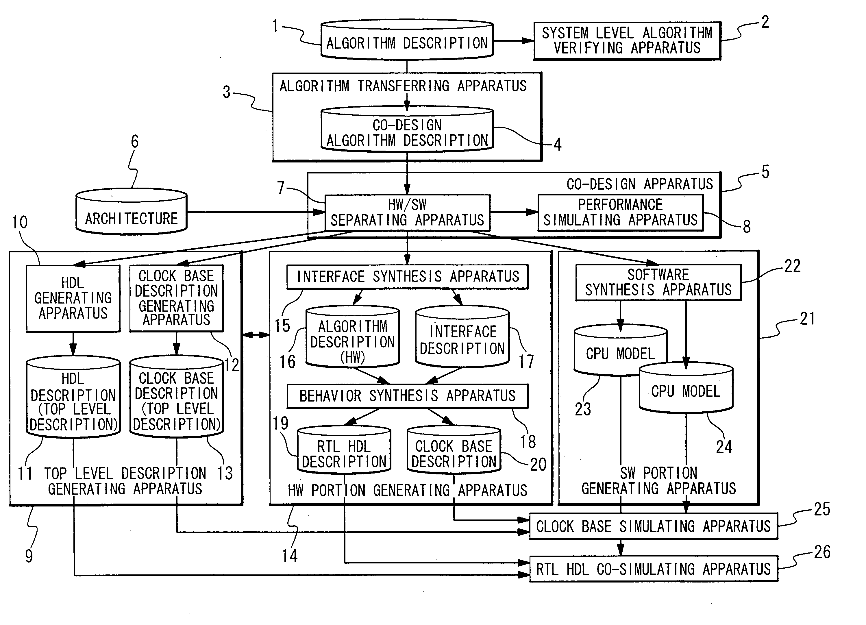
[0060] Embodiments of a circuit designing system and a circuit designing method according to the present invention will be described below with reference to the attached drawings.

[0061]FIG. 1 is block diagram (with flow chart) showing the structure of the circuit designing system (the circuit designing method) according to the present invention.

[0062] The circuit designing system includes a system level algorithm verifying apparatus 2, an algorithm transferring apparatus 3, a co-design apparatus 5, a top level description generating apparatus 9, a hardware (HW) portion generating apparatus 14, a software (SW) portion generating apparatus 21. A clock base simulating apparatus 25 and a RTL HDL co-simulating apparatus 26 execute simulations based on data generated by the circuit designing system. Here, the circuit designing system may include the clock base simulating apparatus 25 and the RTL HDL co-simulating apparatus 26.

[0063] The system level algorithm verifying apparatus 2 veri...


PUM


Abstract

A circuit designing method includes steps (a) to (d). The step (a) separates a first algorithm description for a simulation into a hardware portion describing hardware and a software portion describing software, and generating a design data automatically, wherein the design data includes behavior data, architecture data, mapping data and address data. The step (b) generates a first clock base description automatically based on the design data, wherein the first clock base description describes relation between the hardware portion and the software portion. The step (c) generates a second clock base description automatically based on the design data, wherein the second clock base description describes the hardware portion. The step (d) generates a first CPU model automatically based on the design data, wherein the first CPU model describes the software portion. Here, the first clock base description, the second clock base description and the first CPU model are used for verifying the design data.

Description

BACKGROUND OF THE INVENTION [0001] 1. Field of the Invention [0002] The present invention relates to a circuit designing method and a circuit designing system for designing a large scale circuit. [0003] 2. Description of the Related Art [0004] Recently, the requirement for developing the multi processing system which is composed of ASIC, CPU, memory and so on is rising. When designing such a system, it makes the algorithm (the algorithm description) which the processing operation of the whole system was produced with the hand. Then, first, this algorithm description is verified. Next, it divides into the part which realizes the algorithm description is separated into one part which will be realized by the hardware such as ASIC and another part which will be realized by the software. After that, as for the part of the hardware (HW), RTL HDL description is produced. As for the part of the software (SW), CPU model is produced. Moreover, after producing top level HDL description, a simu...

Claims


Application Information

Patent Timeline
IPC IPC(8): G06F9/45G06F17/50G06G7/62
CPCG06F17/5045G06F17/5022G06F30/30G06F30/33G06F30/3308
Inventor SATO, KOICHISHIBUYA, HIROSHIKUROSAKA, HITOSHI
Owner NEC ELECTRONICS CORP
Why Eureka
Try Eureka