
Low-cost flexible film package module and method of manufacturing the same

Active Publication Date: 2005-02-24
SAMSUNG ELECTRONICS CO LTD
View PDF14 Cites 21 Cited by
  • Summary
  • Abstract
  • Description
  • Claims
  • Application Information

AI Technical Summary

Benefits of technology

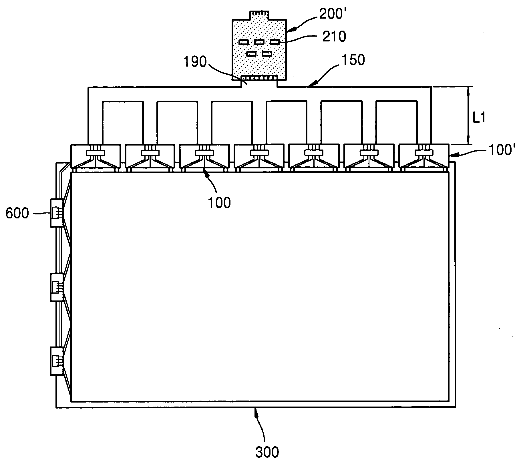
[0015] Exemplary embodiments of the present invention provide a lower-cost flexible film package module in which a tape film used in the flexible film package is formed from a lower-cost flexible printed circuit (FPC) insulating substrate in combination with a polyimide insulating substrate and a method of manufacturing such lower-cost flexible film package modules.
[0021] The printed circuit board can have a smaller width than that of the lower-cost input terminal connecting portion, each of the semiconductor package main bodies can be a tape carrier package and each of the semiconductor package main bodies can be a chip on film package. The exemplary flexible film package modules of the present invention may use a tape film, which combines a first insulating substrate formed of a polyimide material and a second insulating substrate formed of a material that is less expensive than that of the first insulating substrate. Thus, the production costs associated with the flexible film package module can be reduced.

Problems solved by technology

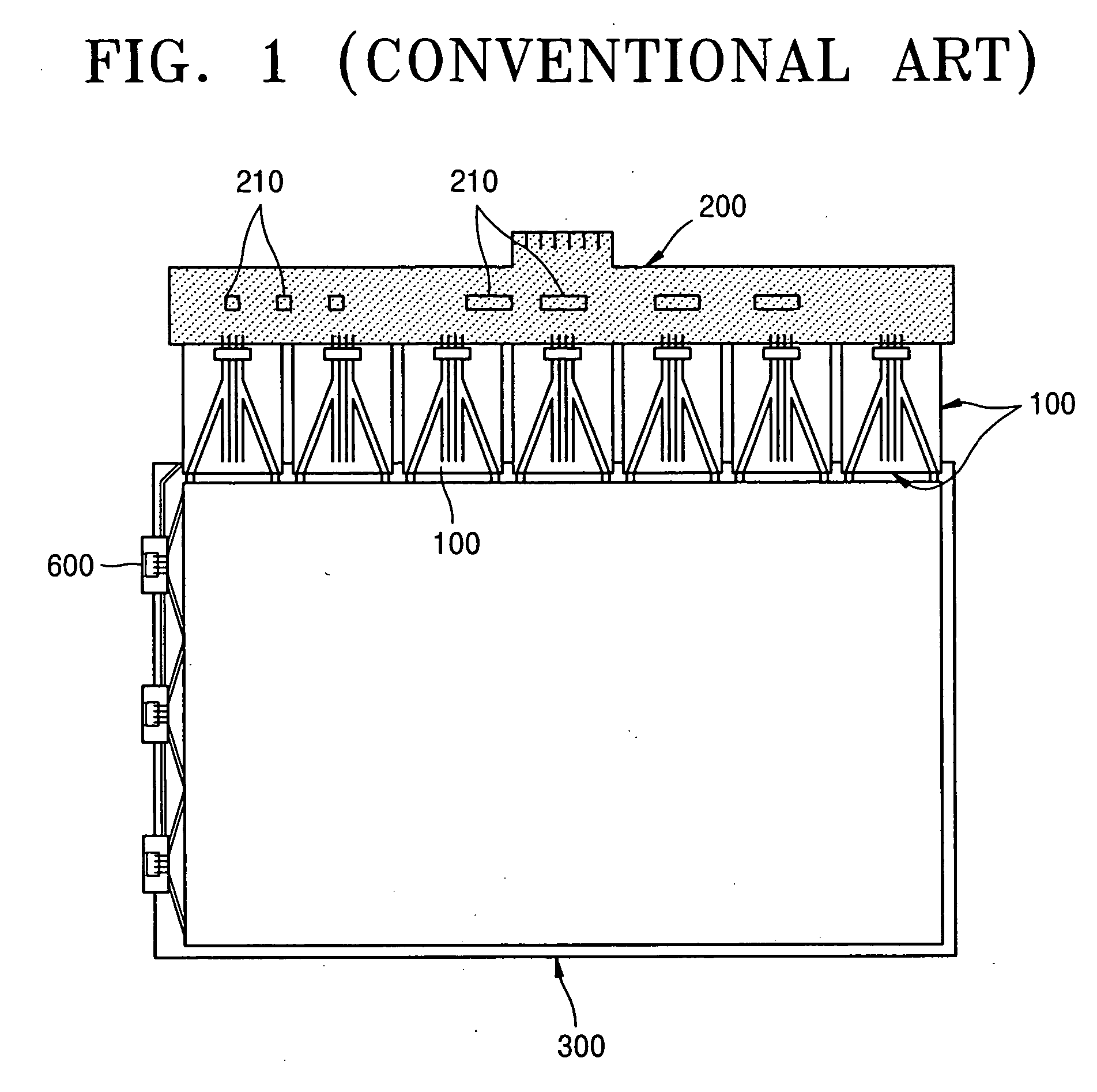
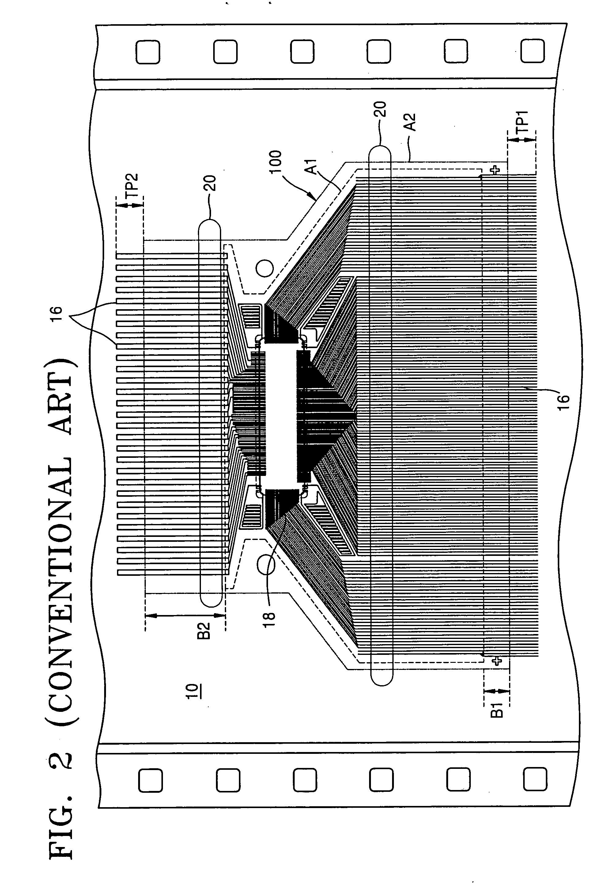
A conventional flexible film package is disclosed in U.S. Pat. No. 6,061,246, dated May 9, 2000, entitled “Microelectric Package Including Flexible Layers and Flexible Extensions, and Liquid Crystal Display Modules Using the Same.” However, conventional flexible film packages have certain limitations.
For example, although the polyimide films used to form the flexible film package tend to have excellent durability and CTE, they also tend to be very expensive so that a semiconductor package manufacturing process that uses a polyimide film will tend to be more costly than one that does not.

Method used


Image

  • Low-cost flexible film package module and method of manufacturing the same
  • Low-cost flexible film package module and method of manufacturing the same
  • Low-cost flexible film package module and method of manufacturing the same

Examples


Embodiment Construction

[0035] The present invention will now be described more fully with reference to the accompanying drawings, in which exemplary embodiments of the invention are shown. This invention may, however, be embodied in many different forms and should not be construed as being limited to solely the embodiments set forth herein. Rather, these exemplary embodiments are provided so that this disclosure will be thorough and complete, and will fully convey the concept of the invention to those skilled in the art.

[0036] As illustrated in FIG. 4, a lower-cost flexible film package module according to an embodiment of the present invention is comprised of a plurality of semiconductor package main bodies 100 and a lower-cost input terminal connecting portion 150. Each of the semiconductor package main bodies 100 is obtained by reducing by as much as 50% to 67% the length of a conventional flexible film package. For example, while a conventional flexible film package may have a typical length of about...


PUM


Abstract

Provided are a flexible film package module and a method of manufacturing the same that can be adapted for manufacture at lower cost and / or to adapt the characteristics of the flexible film package module for specific applications. The lower-cost flexible film package module includes a tape film that combines both a first insulating substrate, typically formed from a higher-cost polyimide material, and a second insulating substrate, typically formed from an insulating material or materials that are less expensive and / or provide modified performance when compared with the first insulating material. Both the first and second substrates will include complementary circuit patterns that will be electrically and physically connected to allow the composite substrate to function as a unitary substrate. The first and second substrates will also include connection regions that may be adapted for connection to printed circuit boards and / or electronic devices such as liquid crystal displays.

Description

CROSS-REFERENCE TO RELATED APPLICATIONS [0001] This application claims priority from Korean Patent Application No. 2003-54221, which was filed on Aug. 5, 2003, in the Korean Intellectual Property Office, the disclosure of which is incorporated herein in its entirety by reference. BACKGROUND OF THE INVENTION [0002] 1. Field of the Invention [0003] The present invention relates to a semiconductor device used for a liquid crystal display (LCD) device and, more particularly, to a flexible film package. [0004] 2. Description of the Related Art [0005] In recent years, the rapid development of LCD-related technologies has accelerated the shift to an information-oriented society. In general, data communication electronic devices in which an LCD is utilized are required to be thin, light-weight, and compact for portable use. Thus, new methods of mounting semiconductor chips on semiconductor packages have been proposed for LCD devices. [0006] While micro ball grid array (μ-BGA)-type semicondu...

Claims


Application Information

Patent Timeline
IPC IPC(8): G02F1/13H01L21/60G02F1/1345H01L23/538H05K1/11H05K1/14
CPCG02F1/13452H01L23/5387H05K1/118H05K1/147H05K2201/068H01L2924/07811H05K2201/10681H01L2224/16H01L2924/00G02F1/1345
Inventor KANG, SA-YOONKIM, DONG-HANCHUNG, YE-CHUNG
Owner SAMSUNG ELECTRONICS CO LTD
Learn More