

High frequency semiconductor integrated circuit device, wireless electric unit and wireless communication system
- Summary
- Abstract
- Description
- Claims
- Application Information
AI Technical Summary
Benefits of technology
Problems solved by technology
Method used
Image

Examples
first embodiment
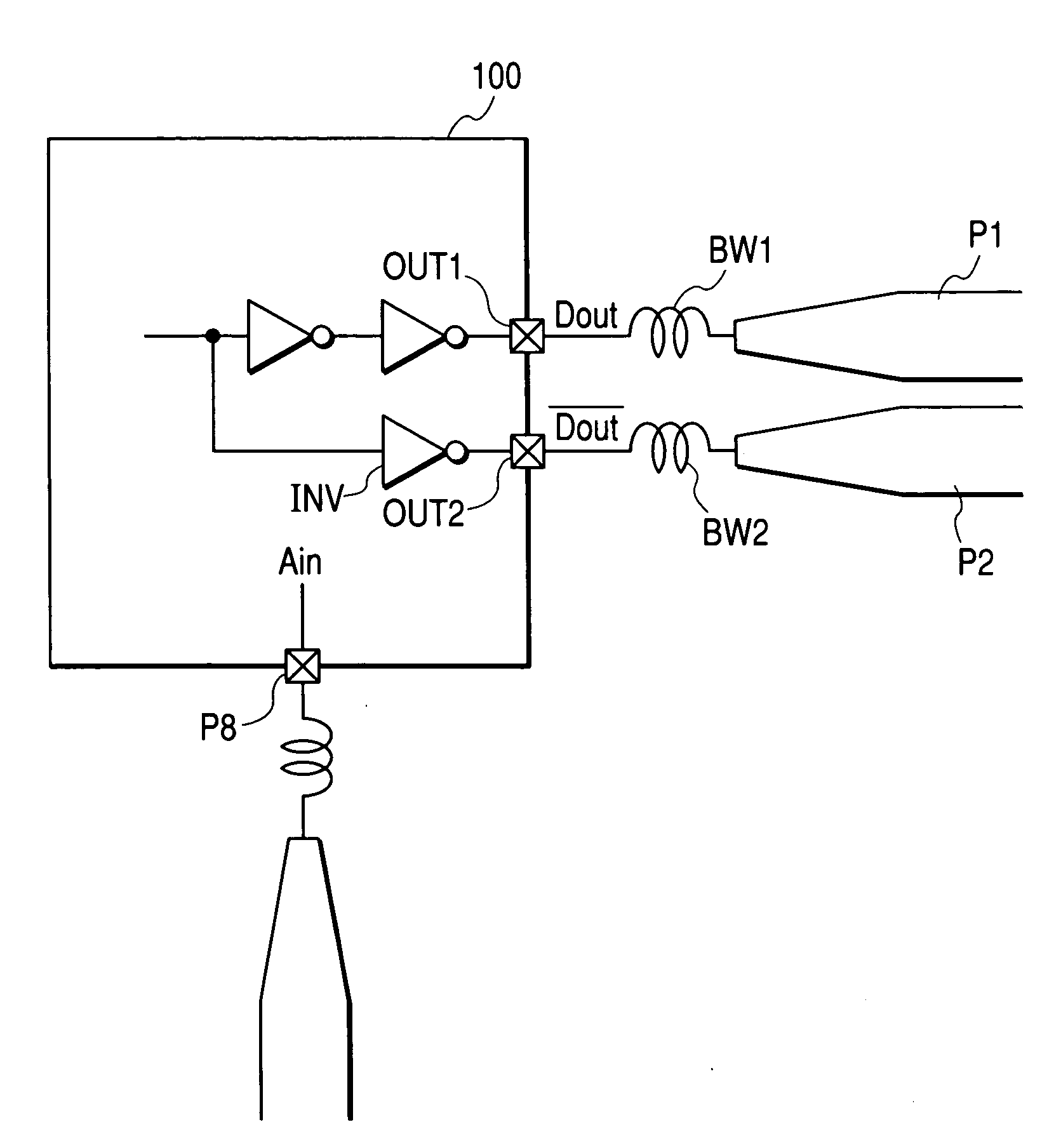
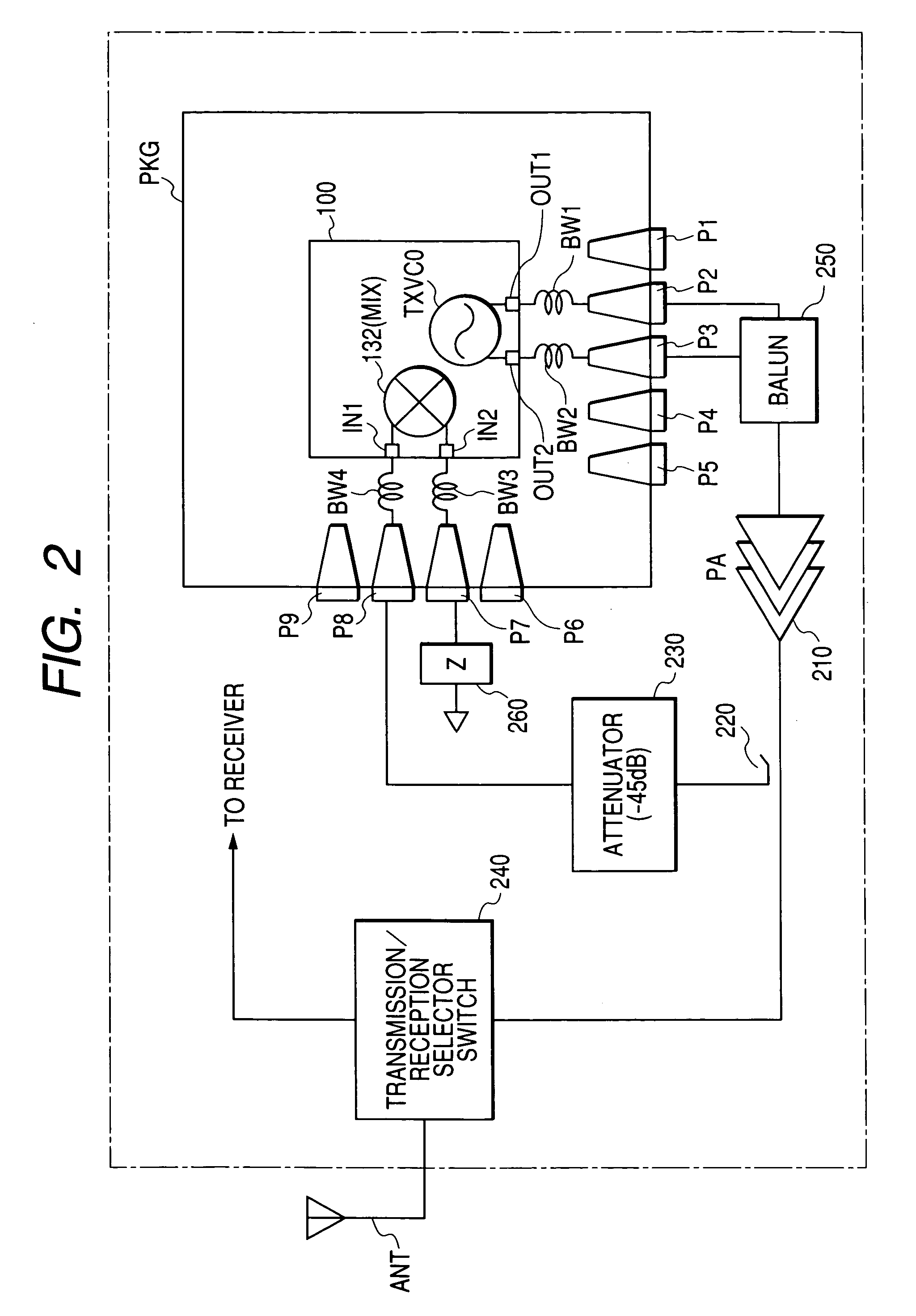
[0050] Next, referring to FIG. 2, the high frequency IC 100 according to the present invention wherein the transmission oscillator TxVCO is provided at its output end with anti-crosstalk measures will be described. Also, the constitution and action of a module mounted with the high frequency IC 100 will be described with reference to FIG. 2.
[0051]FIG. 2 illustrates what is constituted as a module by mounting the following elements over one insulating substrate, such as ceramic substrate: a high frequency IC 100 which constitutes the polar-loop transmitter wireless communication system in FIG. 1; a power amplifier 210; a coupler 220 which detects the output level of the power amplifier 210; an attenuator 230 which attenuates signals detected by the coupler 220; and a transmission / reception selector switch 240. The high frequency IC 100 is mounted as is sealed in a package. In this specification, the high frequency IC 100 sealed in a package is designated as high frequency semiconduct...
second embodiment
[0060] Next, referring to FIG. 3, the high frequency IC 100 according to the present invention wherein the transmission oscillator TxVCO is provided at its output end with anti-crosstalk measures will be described. Also, an RF module mounted with the high frequency IC 100 will be described. In FIG. 3, the same regions and circuits as in FIG. 2 will be marked with the same codes, and duplicate description will be omitted.
[0061] As mentioned above, the first embodiment is provided with the output terminal P3 for transmit signals in opposite phase. In the second embodiment, alternatively, an equivalent impedance circuit 261 is sealed in the package PKG of the high frequency IC. The equivalent impedance circuit 261 has an impedance equivalent to the impedance on the side of the output terminal P2 for transmit signals. That is, the equivalent impedance circuit 261 has an impedance equivalent to the impedance between the other end of the bonding wire BW1 connected with one output terminal...
PUM
 Abstract
Description
Claims
Application Information