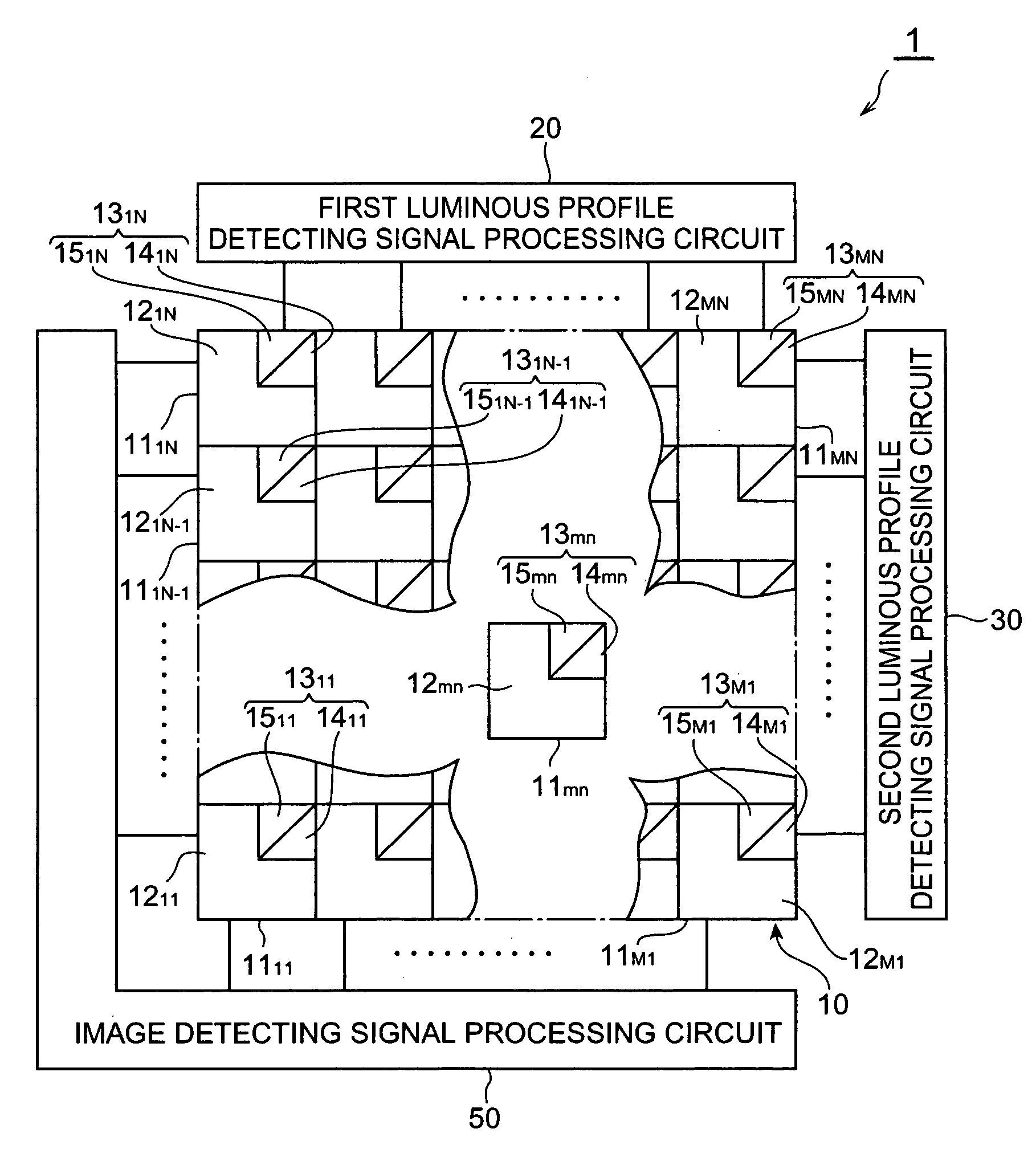
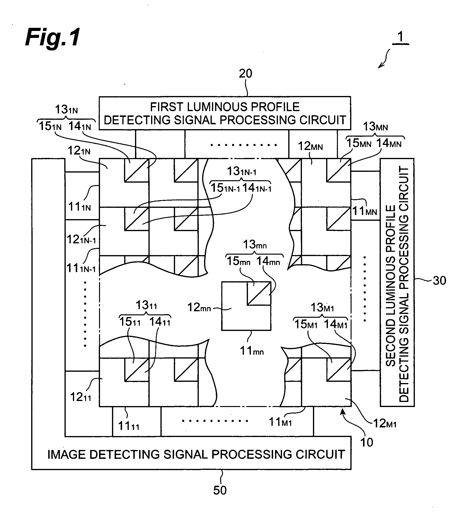
[0006] In the imaging device according to the present invention, light incident on one pixel is detected by each of the first photosensitive portion and the second photosensitive portion that configure the pixel concerned, and the output corresponding to the
light intensity is gained for every photosensitive portion. The image detecting element reads out the output from the first photosensitive portion and detects an image on the basis of the output concerned. Furthermore, the luminous profile detecting element reads out the output from the second photosensitive portion and detects the luminous profiles in the first direction and the second direction in the two-dimensional array on the basis of the output concerned. As described above, since one pixel is configured by the first photosensitive portion and the second photosensitive portion, it is possible to detect both an image and two-dimensional positions where light is incident.
[0007] Furthermore, it is preferable that a wire for leading the outputs from the first photosensitive portions to the image detecting element and a wire for leading the outputs from the second photosensitive portions to the luminous profile detecting element are disposed so as to extend between the pixels. In the case of the above construction, each of the wires will not prevent light from being incident to the first photosensitive portions and the second photosensitive portions, thus suppressing a detection sensitivity reduction.
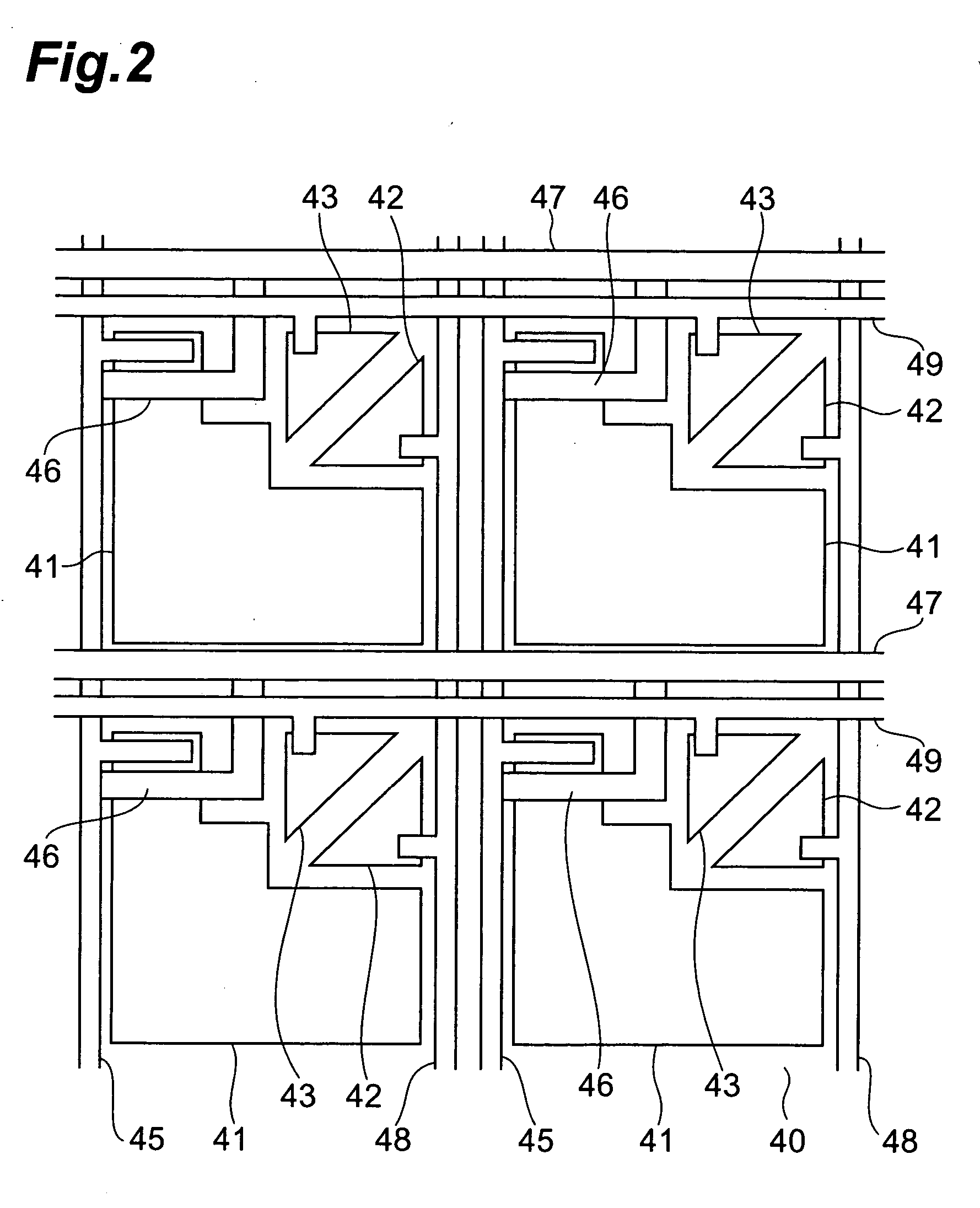
[0008] Still furthermore, it is preferable that the second photosensitive portion contains a plurality of photosensitive portions which are arranged so as to be adjacent to one another on the same plane, the photosensitive portions on one side, amongst the plurality of photosensitive portions contained in the second photosensitive portions, are electrically connected to each other across the plurality of pixels arrayed in the first direction in the two-dimensional array; and the photosensitive portions on the other side, amongst the plurality of photosensitive portions contained in the second photosensitive portions, are electrically connected to each other across the plurality of pixels arrayed in the second direction in the two-dimensional array. In the case of the above construction, light incident to second photosensitive portion is detected by each of the photosensitive portions contained in the second photosensitive portion concerned, and
electric current corresponding to the
light intensity sensed by each photosensitive portion is outputted. Since the photosensitive portions on one side are electrically connected to each other across the plurality of pixels arrayed in the first direction in the two-dimensional array, electric currents from the photosensitive portions on one side are thereafter transmitted to the first direction. Furthermore, since the photosensitive portions on the other side are electrically connected to each other across the plurality of pixels arrayed in the second direction in the two-dimensional array, electric currents from the photosensitive portions on the other side are thereafter transmitted to the second direction. As described above, the electric currents from the photosensitive portions on one side are transmitted in the first direction, and the electric currents from the photosensitive portions on the other side are transmitted in the second direction, so that both of the luminous profile in the first direction and the luminous profile in the second direction are obtained independently. As a result, fast detection of the two-dimensional positions of the incident light becomes possible with an extremely simple structure that a plurality of photosensitive portions are arranged in one pixel.
[0009] Furthermore, it is preferable that a wire for electrically connecting the photosensitive portions on one side, amongst the plurality of photosensitive portions contained in the second photosensitive portions, to each other across the plurality of pixels arrayed in the first direction, is disposed so as to extend in the first direction between the pixels, and a wire for electrically connecting the photosensitive portions on the other side, amongst the plurality of photosensitive portions contained in the second photosensitive portions, to each other across the plurality of pixels arrayed in the second direction is disposed so as to extend in the second direction between the pixels. In the case of the above construction, each of the wires will not prevent light from being incident to the photosensitive portions, thus suppressing a detection sensitivity reduction.
[0010] Still furthermore, it is preferable that the second photosensitive portion outputs an
electric current corresponding to the intensity of incident light, and the luminous profile detecting element comprises: a first luminous profile detecting
shift register for sequentially reading electric currents in the second direction, the electric currents being from groups of the photosensitive portions on one side which are electrically connected across the plurality of pixels arrayed in the first direction; a second luminous profile detecting
shift register for sequentially reading electric currents in the first direction, the electric currents being from groups of the photosensitive portions on the other side which are electrically connected across the plurality of pixels arrayed in the second direction; a first integrating circuit for sequentially receiving the electric currents from each of the groups of photosensitive portions on one side, the electric currents being sequentially read by the first luminous profile detecting
shift register, and converts the electric currents into voltages; and a second integrating circuit for sequentially receiving the electric currents from each of the groups of photosensitive portions on the other side, the electric currents being sequentially read by the second luminous profile detecting shift register, and converts the electric currents into voltages. In the case of this construction, the luminous profile in the first direction and the luminous profile in the second direction can be obtained with an extremely simple structure.
[0011] Furthermore, it is preferable that the first photosensitive portion outputs an
electric current corresponding to the intensity of incident light, and the
image detector comprises a first image detecting shift register for sequentially reading electric currents from the first photosensitive portions in the first direction; and second image detecting shift register for sequentially reading electric currents in the second direction, the electric currents being sequentially read by first image detecting shift register. In the case of this construction, the image can be obtained with an extremely simple structure.

