Ion Milling Device, Sample Processing Method, Processing Device, and Sample Drive Mechanism

Inactive Publication Date: 2012-11-29
HITACHI HIGH-TECH CORP
View PDF4 Cites 25 Cited by
  • Summary
  • Abstract
  • Description
  • Claims
  • Application Information

AI Technical Summary

Benefits of technology

[0018]With the present invention, by continuously varying the ion beam irradiation angle, a smooth processed surface that is not dependent on the material or the ion beam irradiation angle even for composite materials may be obtained. In addition, by providing an ion milling device with an electron irradiation system capable of irradiating a sample with an electron beam and a function for detecting and displaying

Problems solved by technology

With sample surfaces prepared by a mechanical polishing method for the purpose of sample internal structure observation, sometimes fine

Method used


Image

  • Ion Milling Device, Sample Processing Method, Processing Device, and Sample Drive Mechanism
  • Ion Milling Device, Sample Processing Method, Processing Device, and Sample Drive Mechanism
  • Ion Milling Device, Sample Processing Method, Processing Device, and Sample Drive Mechanism

Examples


embodiment 1

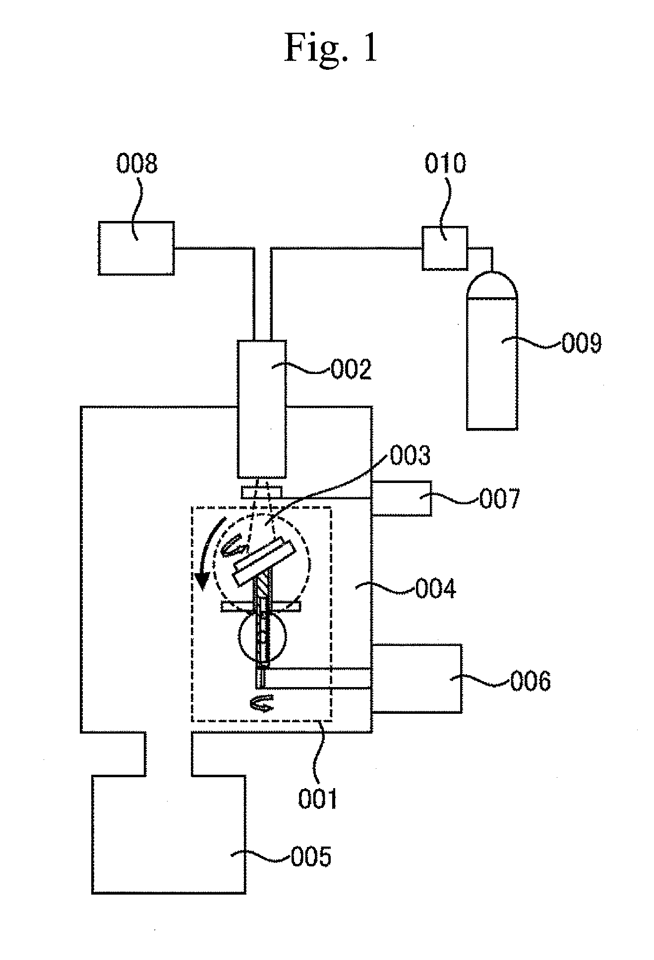
[0031]FIG. 1 is a diagram showing one embodiment of an ion milling device to which the present invention is applied. It comprises: a sample stage 006 equipped with a sample tilting / rotating mechanism 001 according to the present invention that is capable of continuously varying the irradiation angle of an ion beam with which a sample is irradiated, and which is shown enclosed by broken lines in FIG. 1; an ion source 002; a sample chamber 004; an evacuating system 005; an ion current measurement device 007; a high-voltage unit 008; and a gas supply source 009.

[0032]The sample tilting / rotating mechanism 001 of the present embodiment is disposed within the sample chamber 004 via the sample stage 006. The sample chamber 004 has the interior of the sample chamber controlled to atmospheric pressure or a vacuum by the evacuating system 005, and is capable of holding that state.

[0033]The ion source 002 refers to an irradiation system comprising all the elements for emitting an ion beam 003....

embodiment 2

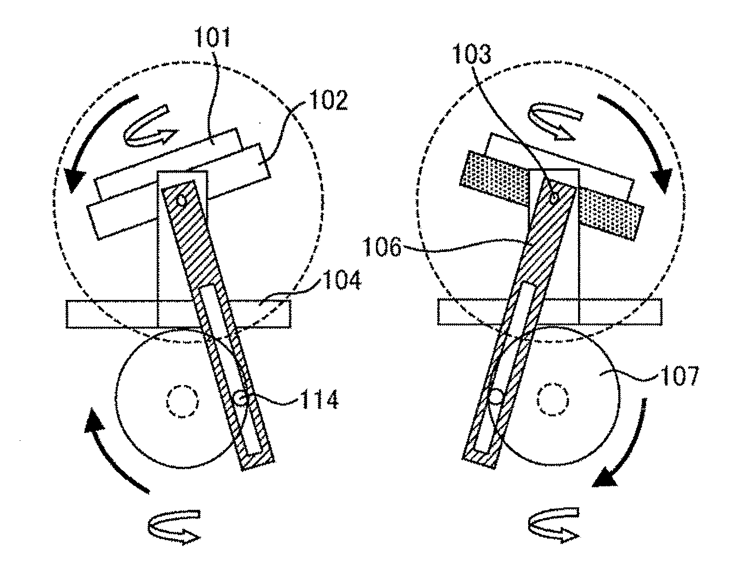
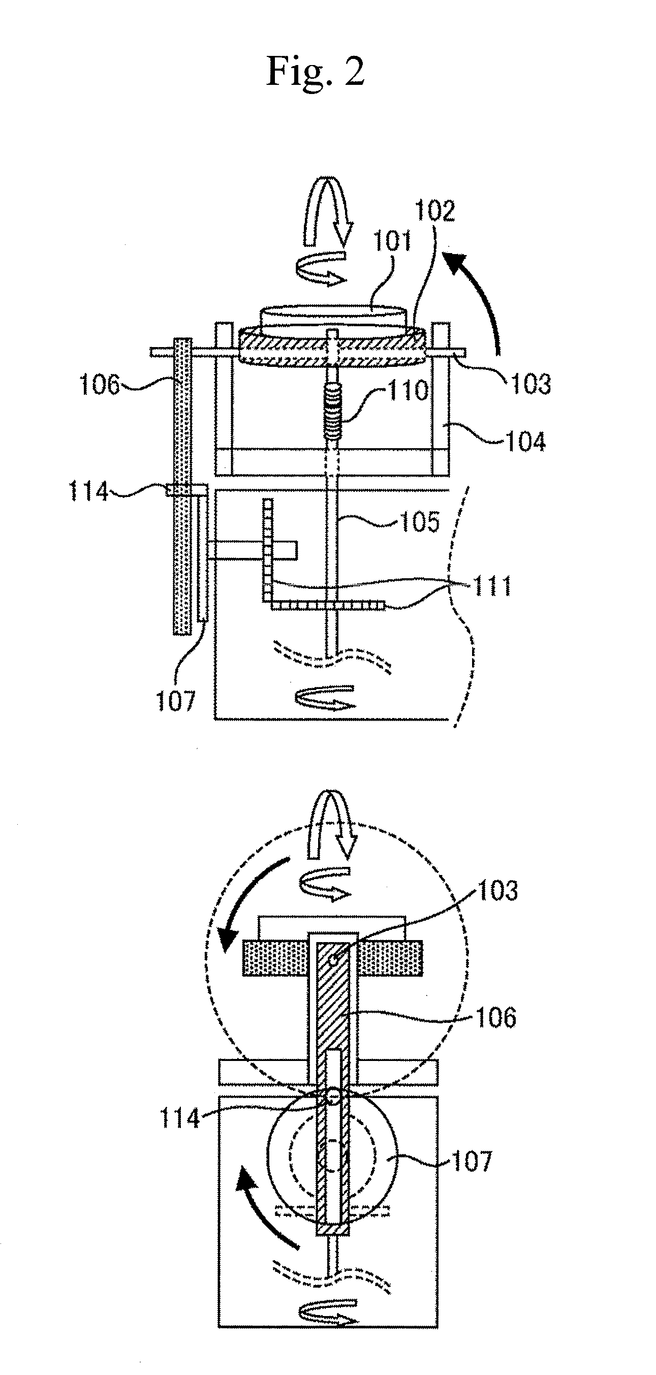
[0043]FIG. 5 is a diagram showing another embodiment of the present invention. It is an illustrative diagram regarding the angle at which the sample is irradiated with the ion beam 003, which is varied continuously by means of the sample rotating / tilting mechanism 001, in other words, sample tilt angle (θ) in the context of the present invention. The range for sample tilt angle (θ) may be altered by having the range of motion of the drive arm 106 be variable.

[0044]Specifically, by disposing the pin 114 attached to the rotating plate 107 that drives the drive arm 106 towards the inner side of the rotating plate 107, or by making the rotating plate 107 smaller, sample tilt angle (θ1) 108 may be decreased as shown in FIG. 5(a). In addition, by disposing the pin 114 attached to the rotating plate 107 that drives the drive arm 106 towards the outer side of the rotating plate 107, or by making the rotating plate 107 bigger, sample tilt angle (θ2) 109 may be increased as shown in FIG. 5(b)...

embodiment 3

[0049]FIG. 7 is a diagram showing an embodiment of end point detection of processing of an ion milling device of the present invention.

[0050]For the present embodiment, a description is provided with respect to a case where an ion milling device according to the present invention is provided with SEM functionality.

[0051]SEM functionality comprises basic functions of a common SEM comprising a secondary electron detector 017 and a backscattered electron detector 013 for detecting signals of secondary electrons 015 and backscattered electrons 016, etc., emitted from the sample 101 when the sample 101 is irradiated with an electron beam 014 by an electron gun 012, wherein the signals are displayed as a two-dimensional image, and so forth.

[0052]An ion milling / SEM control system unit 018 comprises a function of controlling the above-mentioned basic functions of a common SEM as well as displaying the image brightness of a two-dimensional image as a line profile, and a function of controlli...


PUM

PropertyMeasurementUnit
Distanceaaaaaaaaaa

Abstract

In view of the above-mentioned problems, an object of the present invention is to provide a processing method that is not dependent on the material or the ion beam irradiation angle. In order to achieve the object above, the present invention provides a processing device that processes a sample by irradiating the sample with an ion beam, the processing device comprising a sample tilting/rotating mechanism that rotates/tilts the sample relative to the ion beam, wherein the sample rotating mechanism comprises a rotating shaft that rotates the sample relative to the ion beam, and a tilting shaft that is orthogonal to the rotating shaft and that tilts the sample relative to the ion beam, the sample rotating mechanism being adapted to simultaneously perform the rotating and tilting of the sample.

Description

TECHNICAL FIELD[0001]The present invention relates to an ion milling device and a scanning electron microscope sample processing method, and, more particularly, to an ion milling device and a scanning electron microscope sample processing method for preparing a sample to be observed / analyzed using a scanning electron microscope or an EBSP (Electron BackScatter diffraction Pattern) method, etc.BACKGROUND ART[0002]Along with the rapid advancements in packaging technology for electronic devices in recent years, constituent components of electronic components have also become smaller and denser, and SEM observation / analysis needs for the internal structures thereof are growing rapidly.[0003]With sample surfaces prepared by a mechanical polishing method for the purpose of sample internal structure observation, sometimes fine structures are unobservable / unanalyzable due to deformation, polishing damage, or drooping caused by the stress exerted during polishing. To address this, ion millin...

Claims


Application Information

Patent Timeline
IPC IPC(8): G21K5/10
CPCH01J37/20H01J37/28H01J37/3056H01J2237/3114H01J2237/20214H01J2237/20242H01J2237/20207B23K15/00G01N1/28H01J37/30
Inventor NAKAJIMA, RIEKUROSAWA, KOICHITAKASU, HISAYUKI
Owner HITACHI HIGH-TECH CORP
Why Eureka
Try Eureka