Nitride semiconductor device, its manufacturing method, and semiconductor optical apparatus

Inactive Publication Date: 2005-02-24
SHARP KK +1
View PDF1 Cites 95 Cited by
  • Summary
  • Abstract
  • Description
  • Claims
  • Application Information

AI Technical Summary

Benefits of technology

[0009] In the light of the above problems, the present invention aims at providing a nitride composite semiconductor laser element internally containing minimi

Problems solved by technology

Generation of the above problems is caused by the crystalline defect, i.e., the “

Method used


Image

  • Nitride semiconductor device, its manufacturing method, and semiconductor optical apparatus
  • Nitride semiconductor device, its manufacturing method, and semiconductor optical apparatus
  • Nitride semiconductor device, its manufacturing method, and semiconductor optical apparatus

Examples


first embodiment

OF THE PRESENT INVENTION

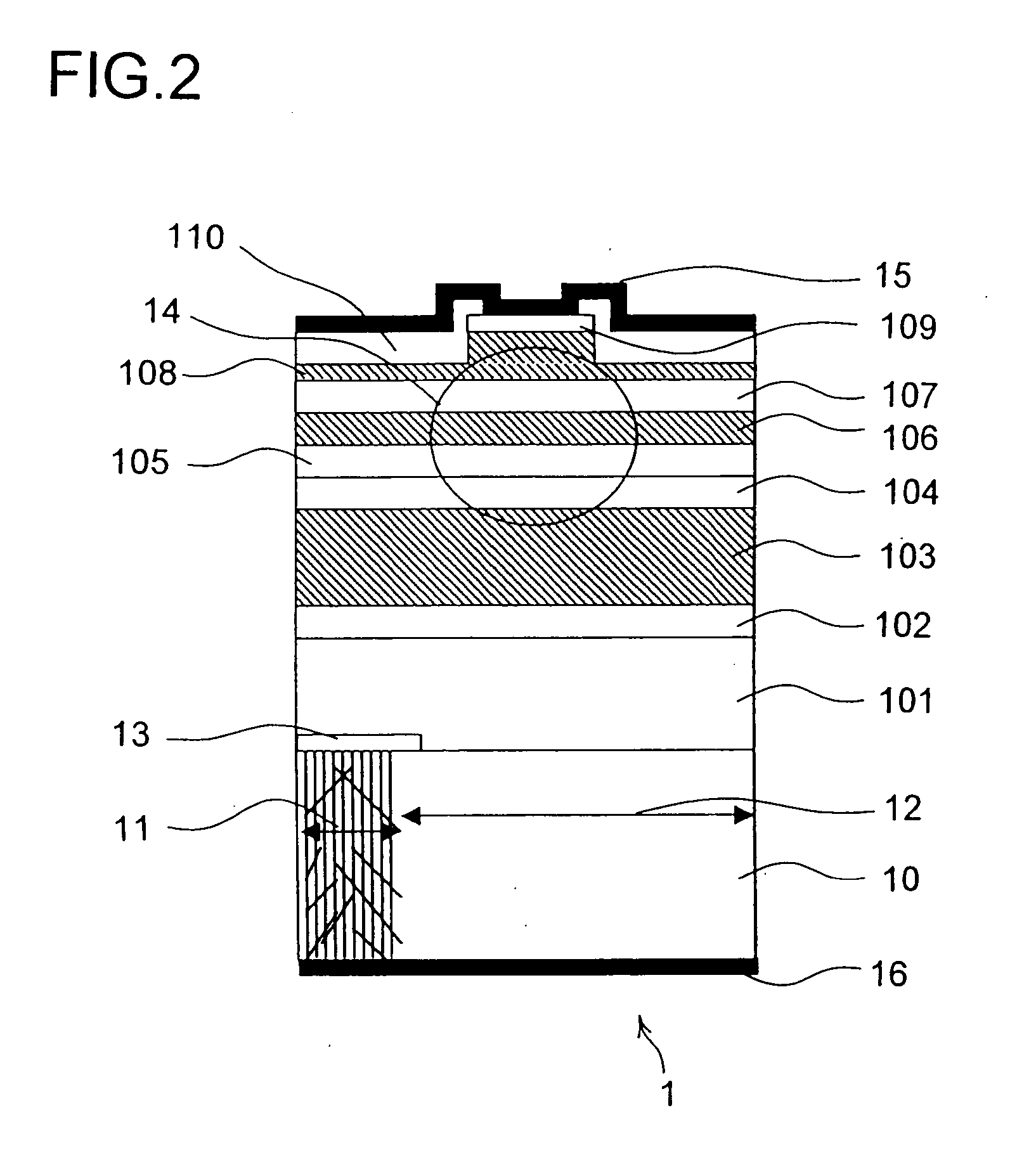
[0082] Referring now to the accompanying drawings, the first embodiment of the present invention for manufacturing a nitride composite semiconductor laser element is described below, wherein the nitride composite semiconductor laser element is produced by applying an n-type GaN composite substrate incorporating the above-referred regions concentrated with the “dislocated” crystalline defect and the above-referred “high-luminescence regions”. FIG. 2 is a cross-sectional view exemplifying the constitution of the nitride-composite semiconductor laser element 1 according to the first embodiment of the present invention. Note that illustration of the “high-luminescence region” is not shown in FIG. 2.

[0083] [Process for Forming “Growth Inhibiting Films”]

[0084] First, a growth inhibiting film 13 shown in FIG. 2 is formed on the surface of the n-type GaN composite semiconductor substrate 10. The growth inhibiting film 13 is formed so as to cover a “dislocation conce...

second embodiment

OF THE PRESENT INVENTION

[0125] Referring now to the accompanying drawings, the second embodiment of the nitride semiconductor laser elements manufactured by applying the n-type GaN composite substrate incorporating those regions concentrated with “dislocation” and those high luminescence regions based on the above formation is described below. Processes for epitaxially growing the nitride semiconductor layers and manufacturing laser elements are identical to those which are performed for the first embodiment of the present invention, and thus, for detailed description of these constituents, refer to the preceding description on the first embodiment, thereby omitting description thereof.

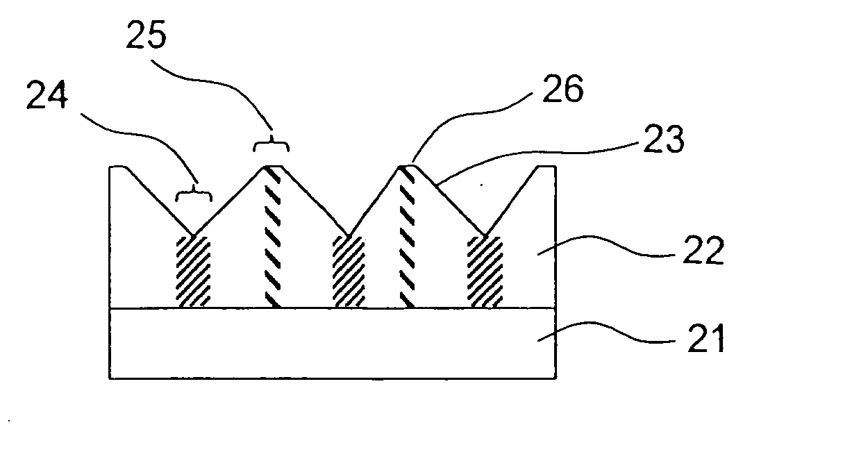
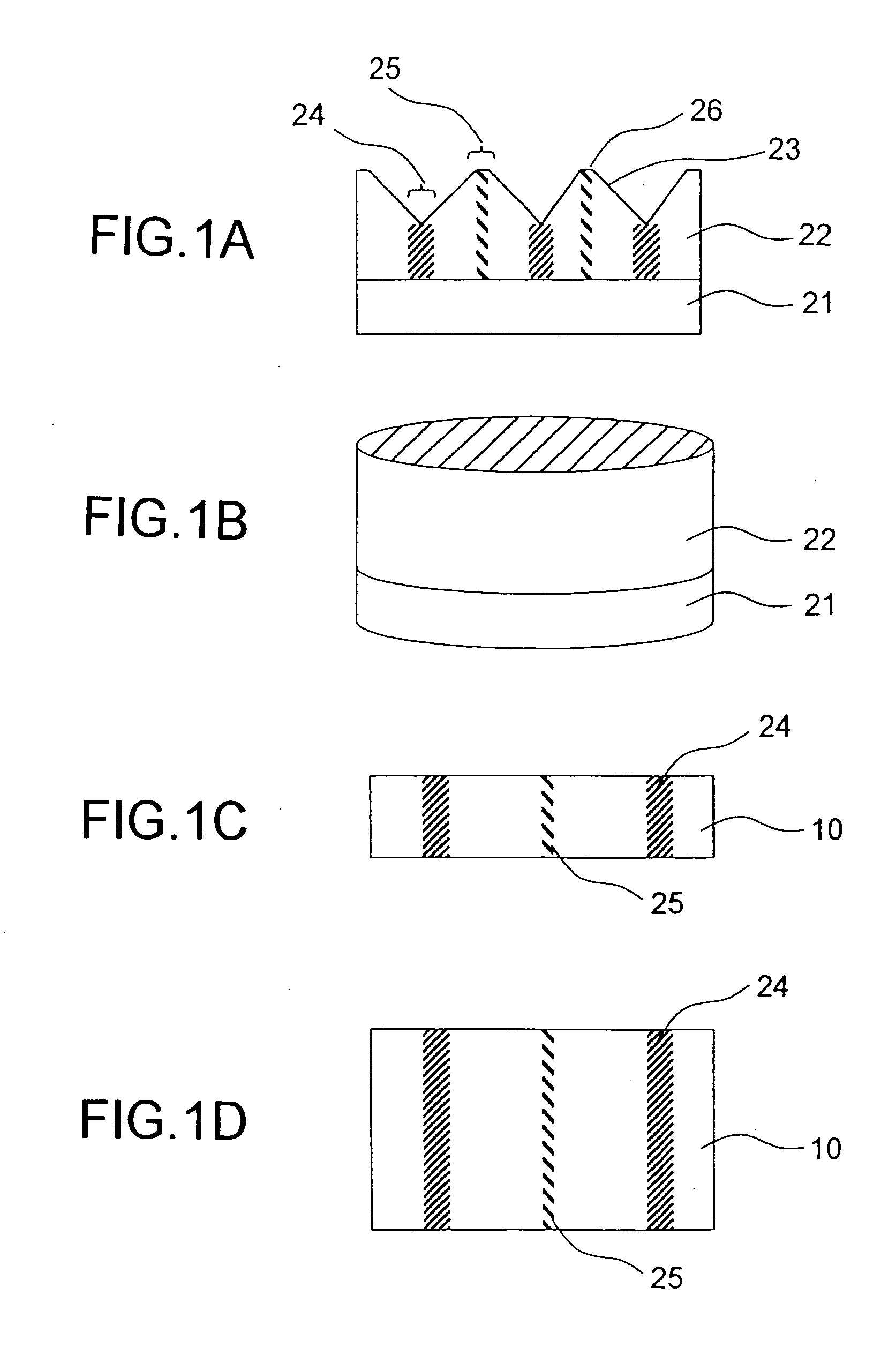
[0126] In the second embodiment, unlike the preceding first embodiment, a growth inhibiting film is formed in order that those regions 24 concentrated with “dislocation” (shown in FIG. 1A to 1D) can fully covered by the growth inhibiting film, and that the growth inhibiting film can be formed on the ...

third embodiment

OF THE PRESENT INVENTION

[0142]FIG. 7 is a schematic cross-sectional view of a semiconductor laser element 3 according to the third embodiment of the present invention. In FIG. 7, the semiconductor laser element 3 of the third embodiment is seen from the light emitting direction. The reference numeral 10 represents an n-type GaN composite substrate, in which a number of dislocation concentrated regions 11 are present. Those portions other than the dislocation concentrated region 11 consist of low-dislocation accommodating regions. Intervals (pitch P) between individual regions 11 are respectively at 400 μm. Within the low dislocation regions, high luminescence regions 25 are present in parallel with the regions 11. A number of nitride semiconductor (epitaxially grown) layers 1000 are formed on the substrate 10. A laser beam guide region 14 is disposed inside of the nitride semiconductor layers. An electrode 15 is formed on the upper surface of the nitride semiconductor layers 1000, w...


PUM


Abstract

A nitride semiconductor laser device with a reduction in internal crystal defects and an alleviation in stress, and a semiconductor optical apparatus comprising this nitride semiconductor laser device. First, a growth suppressing film against GaN crystal growth is formed on the surface of an n-type GaN substrate equipped with alternate stripes of dislocation concentrated regions showing a high density of crystal defects and low-dislocation regions so as to coat the dislocation concentrate regions. Next, the n-type GaN substrate coated with the growth suppressing film is overlaid with a nitride semiconductor layer by the epitaxial growth of GaN crystals. Further, the growth suppressing film is removed to adjust the lateral distance between a laser waveguide region and the closest dislocation concentrated region to 40 μm or more.

Description

TECHNICAL FIELD [0001] The present invention relates to a nitride-composite semiconductor laser element, which is constituted with plural nitride composite semiconductor layers laminated on a nitride-composite semiconductor substrate, and also relates to a method of manufacturing it, while the present invention further relates to a semiconductor optical device using the nitride-composite semiconductor laser element in subject. BACKGROUND ART [0002] Conventionally, from the viewpoint of wave-band constitution and chemical stability, in the field of the III-V family nitride semiconductors consisting of the III family elements such as aluminum (Al), gallium (Ga), and indium (In), and of nitrogen (N) corresponding to one of the V family elements (this will merely be referred to as a GaN composite semiconductor hereinafter), there has been much expectation on the potential utility of this GaN composite semiconductor for its practical application to a light emitting element and a power de...

Claims


Application Information

Patent Timeline
IPC IPC(8): H01L21/20H01S5/02H01S5/323
CPCH01S5/0207H01S5/2231H01S5/3202H01S5/32341H01S2301/173H01S5/2018H01L21/02647H01L21/02389H01L21/02458H01L21/02505H01L21/0254H01L21/0262H01L21/02639H01S5/3013H01S5/0021H01S5/320275
Inventor ITO, SHIGETOSHIYUASA, TAKAYUKIUETA, YOSHIHIROTANEYA, MOTOTAKATANI, ZENPEIMOTOKI, KENSAKU
Owner SHARP KK
Why Eureka
Try Eureka