Apparatus and method for cleaning printed circuit boards

a printed circuit board and cleaning apparatus technology, applied in the field of electronic manufacturing processes, can solve the problems of consuming valuable manufacturing time, circuit board cleaning equipment itself is extremely expensive, and the cleaning of printed circuit boards in such a context is as expensive as it is important, so as to reduce the time consumed by the drying phase portion and optimize the drying

Inactive Publication Date: 2005-03-03
STACH STEVEN R
View PDF80 Cites 4 Cited by
  • Summary
  • Abstract
  • Description
  • Claims
  • Application Information

AI Technical Summary

Benefits of technology

[0019] As will be described in more detail later, the preferred embodiment of the present invention includes a particular, preferred design for its drying manifold which optimizes drying, particularly of such things as printed circuit boards, and thereby reduces the time consumed by the drying phase portion of any cleaning and drying cycle.

Problems solved by technology

Ionic contamination (both positive and negative ions) can cause corrosion if not removed from the printed circuit board.
Cleaning printed circuit boards in such a context is as expensive as it is important.
Not only is present circuit board cleaning equipment itself extremely expensive, but the time involved in cleaning consumes valuable manufacturing time, in an industry where, quite literally, every second counts, if the manufacturer is to be competitive.
Further still, present cleaning equipment suitable for circuit board cleaning operations is either quite large, consuming valuable floor space in manufacturing facilities which tend, because of the nature of the industry, to be quite expensive on a square footage basis, or, in the case of batch cleaners, is smaller, but require very long processing times.
As already alluded, batch cleaners, while taking up much less space, consume many multiples of processing time than do present in-line cleaners.
Such need is long-felt, yet never fully satisfied.

Method used


Image

  • Apparatus and method for cleaning printed circuit boards
  • Apparatus and method for cleaning printed circuit boards

Examples


Embodiment Construction

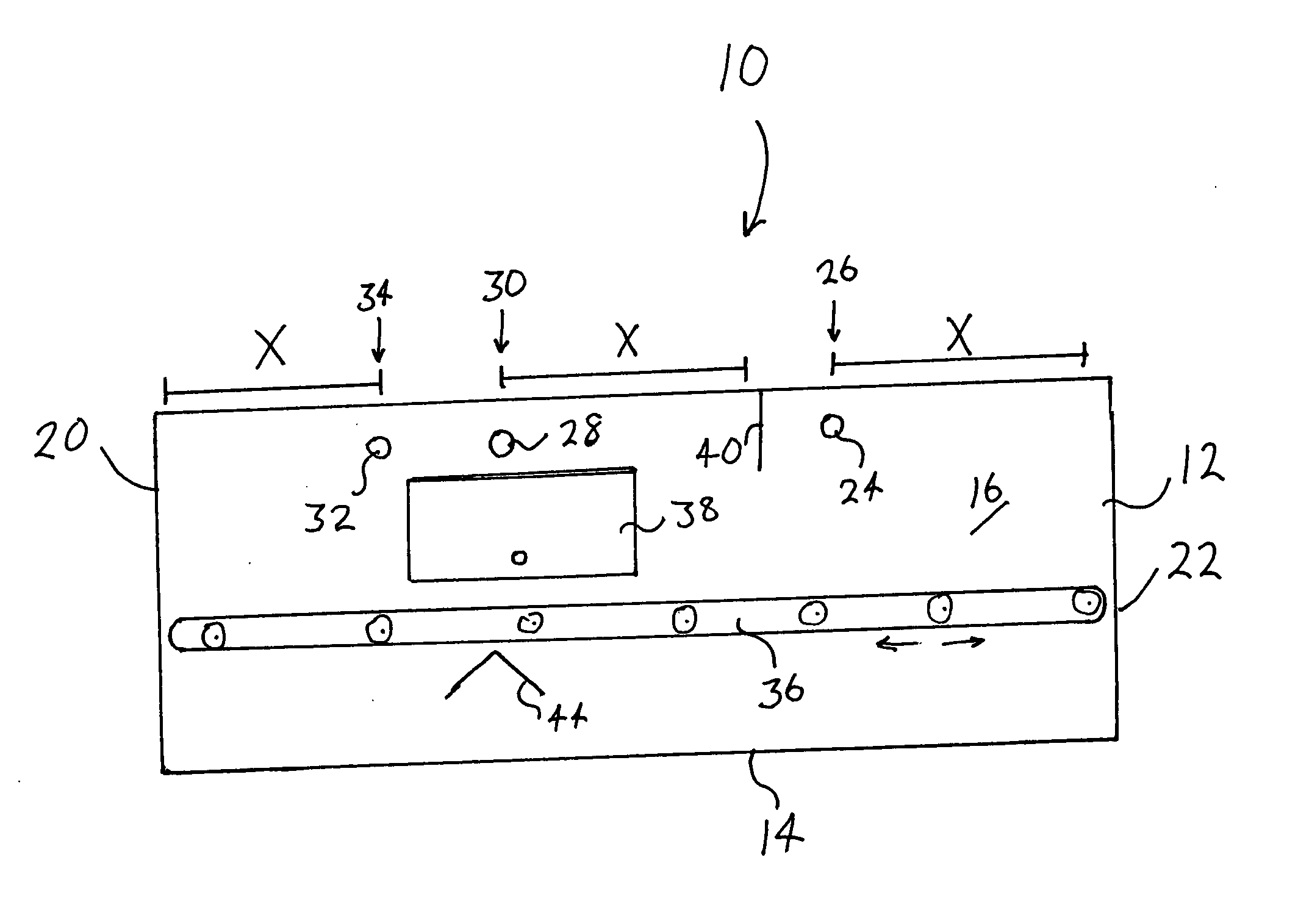
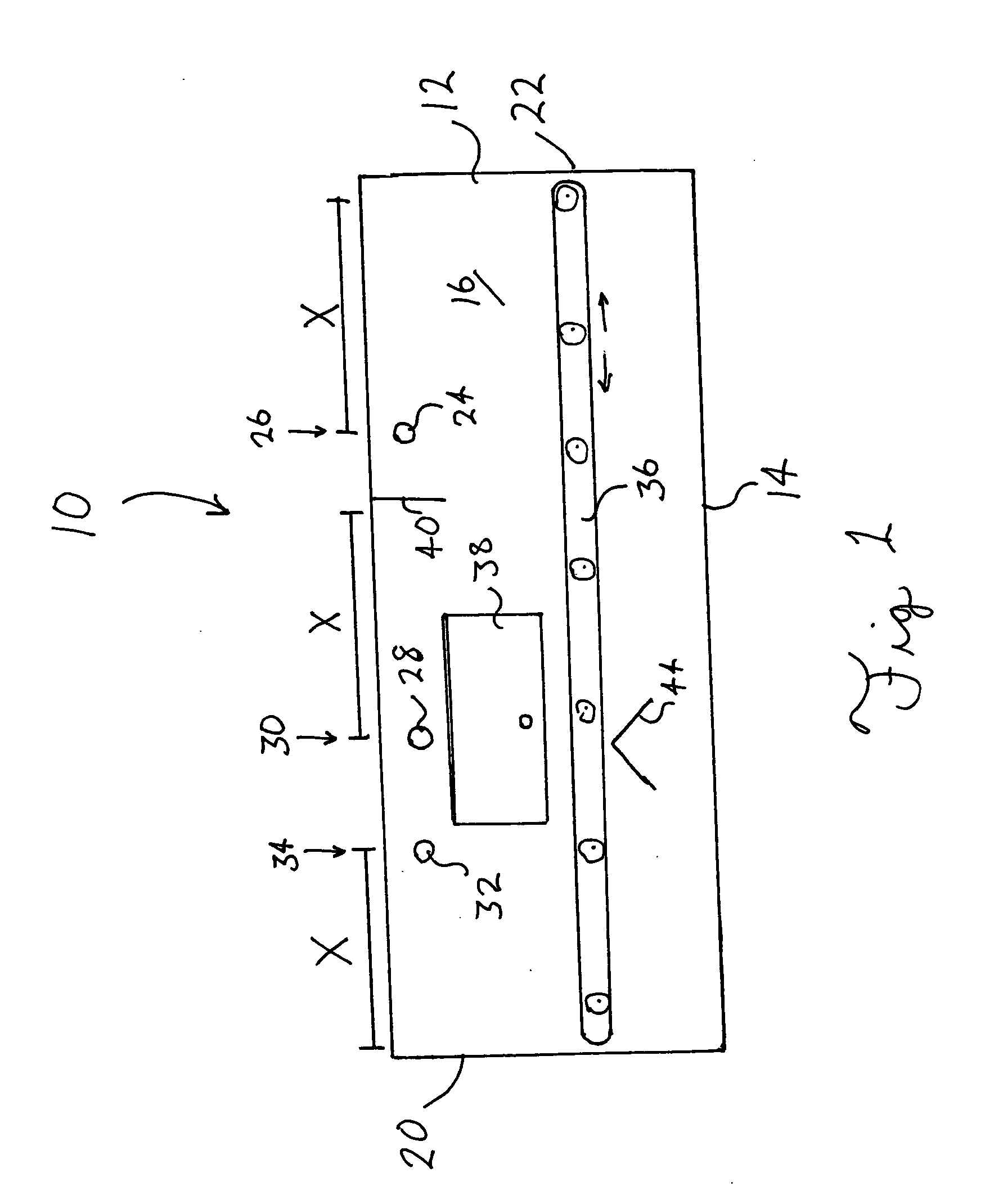
[0021] Referring to FIG. 1, the circuit board cleaning system of the present invention is depicted (somewhat schematically) in general by the reference number 10. System 10 includes an elongate enclosure 12 with a base or floor member 14, side walls 16 (only front side wall visible in drawing), a top or ceiling panel 18. For ease of description, the distal ends of enclosure 12 are (as if viewed from the front side) referred to as the left end (or first end) 20 and the right end (or second end) 22.

[0022] A washing nozzle assembly 24 resides at, and defines a first linear position 26 relative to the long axis of enclosure 12. A drying manifold 28 resides at, and defines a second linear position 30. A rinsing nozzle assembly 32 resides at, and defines a third linear position 34. Suitable designs for washing nozzle assembly 24 and rinsing nozzle assembly 32, as well as the associated pumps, conduits, valves, actuating systems, and distance from work piece parameters are well known in t...


PUM

PropertyMeasurementUnit
sizeaaaaaaaaaa
distanceaaaaaaaaaa
distanceaaaaaaaaaa

Abstract

A highly compact yet fast operating washing and drying system, principally for use in cleaning and drying printed circuit boards after soldering. The system includes a bi-directional conveyor and control systems for moving to-be-processed articles past optimally spaced (for manufacturing facility space savings) washing, rinsing and drying components according to pre-programmed processing profiles (number of passes past washing nozzles, drying jets, etc.).

Description

BACKGROUND OF THE INVENTION [0001] 1. Field of The Invention [0002] Applicant's invention relates to electronic manufacturing processes, and more particularly to the printed circuit board cleaning step which follows the soldering of electronic components onto a circuit board. [0003] 2. Background Information [0004] During the assembly of components on printed circuit wiring boards, soldering fluxes are first applied to the substrate board material to insure that the solder will firmly bond the components to the wiring traces imprinted on the printed circuit board. After soldering, remaining flux residue must be removed. Ionic contamination (both positive and negative ions) can cause corrosion if not removed from the printed circuit board. [0005] Cleaning printed circuit boards in such a context is as expensive as it is important. Not only is present circuit board cleaning equipment itself extremely expensive, but the time involved in cleaning consumes valuable manufacturing time, in...

Claims


Application Information

Patent Timeline
Patent Type & Authority Applications(United States)
IPC IPC(8): B08B3/02H05K3/22H05K3/26
CPCB08B3/022H05K3/227H05K2203/1509H05K2203/075H05K3/26
Inventor STACH, STEVEN R.
Owner STACH STEVEN R
Why Eureka
Try Eureka