Insulated gate transistor incorporating diode

a technology of insulating gate transistor and diode, which is applied in the field of transistors, can solve the problems of reducing the performance of an igbt, the conductible current of the power mosfet is relatively low, and the power mosfet is unsuitable for high current applications, and achieves the effect of improving the recovery characteristics of the diod

Active Publication Date: 2005-03-03
MITSUBISHI ELECTRIC CORP
View PDF17 Cites 145 Cited by
  • Summary
  • Abstract
  • Description
  • Claims
  • Application Information

AI Technical Summary

Benefits of technology

[0019] It is an object of the present invention to effectively improve recovery characteristics of a diode (be also referred to as a diode portion) which serves as a FWD and is inc

Problems solved by technology

Instant release of the energy stored in the L of the motor leads to generation of an electric power which is high enough to degrade performance of an IGBT.
However, a density of a conductible current of the power MOSFET is relatively low, and thus the power MOSFET is unsuitable for high current applications.
Such voltage is too high for a breakdown voltage of a built-in freewheeling diode.
Because of this high breakdown voltage, a barrier which is unsuitable as a freewheeling diode is formed, and thus performance of the IGBT is significantly degraded due to heat generated by the high breakdown voltage applied during freewheeling.
For this reason, while an IGBT is advantageous to a power MOSFET in that flow of a high current in a device is

Method used


Image

  • Insulated gate transistor incorporating diode
  • Insulated gate transistor incorporating diode
  • Insulated gate transistor incorporating diode

Examples


first preferred embodiment

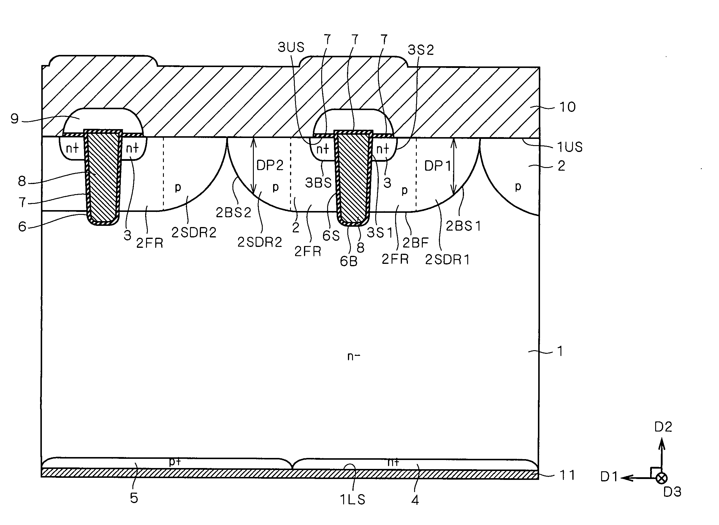
[0069] Features or essences of one IGBT unit (which includes one IGBT unit cell and a diode incorporated therein) of an IGBT device of a trench gate type according to a first preferred embodiment can be understood by reference to a longitudinal sectional view of FIG. 1 about which details will be provided later. The one IGBT unit includes: I) a first semiconductor layer (a p-type base layer or p-type base region in an example given in the present description) 2 of a second conductivity type (p-type in the present example) which is shaped like a well extending from a first main surface 1US of a semiconductor substrate (n−-type substrate or layer in the present example) 1 of a first conductivity type (n-type in the present example) toward an interior of the semiconductor substrate 1 and includes a flat region 2FR including a bottom surface 2BF forming a flat surface substantially parallel to the first main surface 1US, a first side diffusion region 2SDR1 joined to the flat region 2FR,...

second preferred embodiment

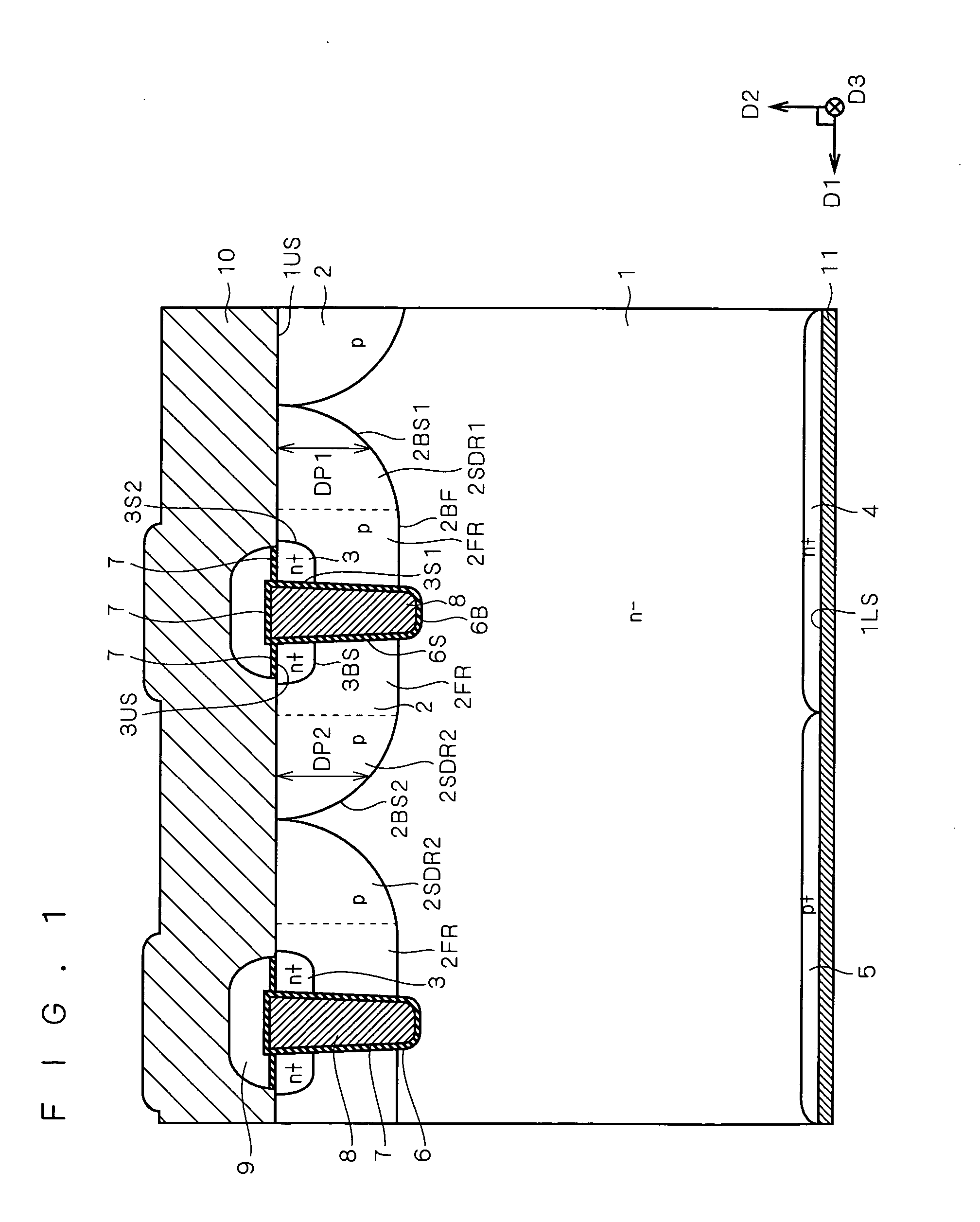
[0084]FIG. 5 is a longitudinal sectional view of a structure of one IGBT unit cell and its surroundings according to one example of a second preferred embodiment. The structure illustrated in FIG. 5 is different from the structure of the IGBT unit cell illustrated in FIG. 1 in that two main trenches 6 pass through the p-type base layer 2 in the first semiconductor layer 2 shaped like a well, so that the flat region 2FR in the first semiconductor layer 2 is sandwiched between the two main trenches 6. The first side diffusion region 2SDR1 is situated just above the n+-type cathode layer 4. The depth DP1 of the bottom surface 2BS1 of the first side diffusion region 2SDR1 is the largest at a joint between the bottom surface 2BS1 and a side surface of one of the two main trenches 6 closer to the first side diffusion region 2SDR1, and gradually decreases as a distance to a joint between the first main surface 1US and the bottom surface 2BS1 decreases, so that the bottom surface 2BS1 forms...

third preferred embodiment

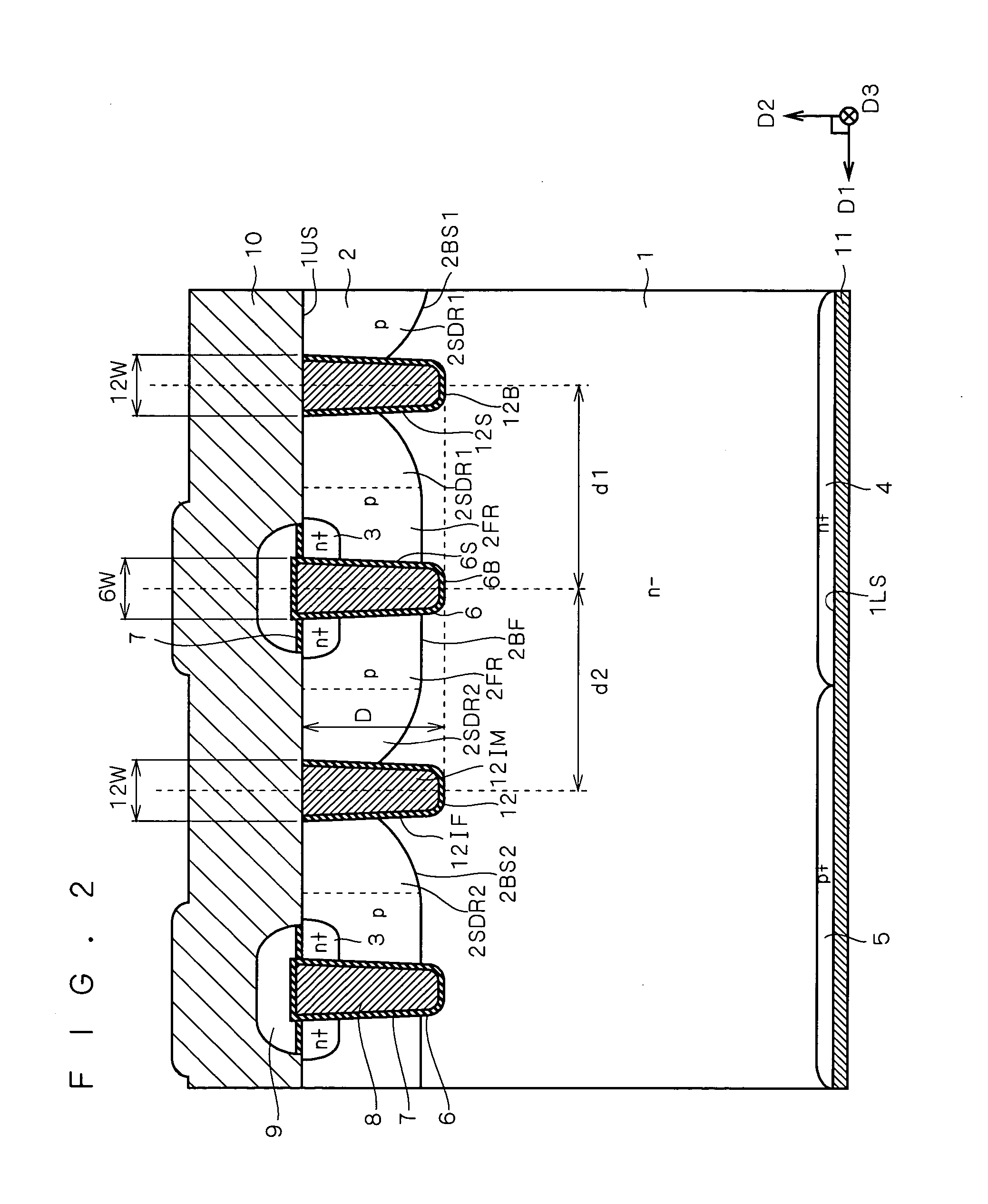
[0091] Essences of a structure according to a third preferred embodiment can be appreciated from a longitudinal sectional view of FIG. 7 about which more details will be provided later. First, (I) a well layer WL of the second conductivity type extending from the first main surface 1US toward an interior of the semiconductor substrate 1 and facing the first side diffusion region 2SDR1 along the first direction D1 while being spaced by a predetermined distance 13W from the first side diffusion region 2SDR1 is further provided. Also, (II) the first main electrode 10 is also situated on an inter-well region 1USWR corresponding to a portion of the first main surface 1US which is sandwiched between a joint between the bottom surface 2BS of the well layer WL and the first main surface 1US and a joint between the bottom surface 2BS1 of the first side diffusion region 2SDR1 and the first main surface 1US. Further, (III) a thin silicide film (a silicide layer containing platinum and silicon,...


PUM


Abstract

A p-type base layer shaped like a well is formed for each of IGBT cells, and a p+-type collector layer and an n+-type cathode layer are formed on a surface opposite to a surface on which the p-type base layer is formed so as to be situated just below the p-type base layer. The p-type base layer of each of the IGBT cells includes a flat region including an emitter region and a bottom surface penetrated by a main trench, and first and second side diffusion regions between which the flat region is interposed. The first side diffusion region is situated just above the n+-type cathode layer and each of the bottom surfaces of the side diffusion regions forms a parabola-shaped smooth curve in longitudinal section. By replacing the p+-type collector layer with the n+-type cathode layer, it is possible to apply features of the above structure to a power MOSFET.

Description

BACKGROUND OF THE INVENTION [0001] 1. Field of the Invention [0002] The present invention relates to a transistor including an insulated gate (MOS structure) (for example, an insulated gate bipolar transistor, a power MOSFET or the like). Additionally, an insulated gate bipolar transistor will hereinafter be also referred to as an “IGBT”, and may be also referred to as a “reverse conducting IGBT”. The present invention relates more particularly to a structure of an insulated gate transistor which has a trench gate structure and incorporates a diode functioning as a freewheeling diode (which will hereinafter be also abbreviated as a “FWD”), and a technique for manufacturing the same. The present invention provides for improvement of recovery characteristics exhibited by the diode incorporated in an insulated gate transistor during an operation mode of the diode. [0003] 2. Description of the Background Art [0004] In power electronics for driving a motor or the like, under a condition ...

Claims


Application Information

Patent Timeline
IPC IPC(8): H01L21/331H01L21/28H01L21/336H01L27/04H01L29/06H01L29/41H01L29/739H01L29/78H02M7/5387
CPCH01L29/0696H01L29/1095H01L29/407H01L29/66348H01L29/7813H01L29/7803H01L29/7805H01L29/7806H01L29/7397H01L29/7812H01L2924/13055
Inventor TAKAHASHI, HIDEKI
Owner MITSUBISHI ELECTRIC CORP
Why Eureka
Try Eureka