
Integrated circuit device with embedded passive component by flip-chip connection and method for manufacturing the same

a technology of integrated circuit devices and passive components, which is applied in the direction of semiconductor devices, electrical devices, semiconductor/solid-state device details, etc., can solve the problems of poor quality and yield of ic chips, inability to precisely control the resistance of embedded passive components in chips, and difficulty in manufacturing embedded passive components inside ic chips. achieve the effect of reducing fabrication costs and high yield

Active Publication Date: 2005-03-03
ADVANCED SEMICON ENG INC
View PDF5 Cites 58 Cited by
  • Summary
  • Abstract
  • Description
  • Claims
  • Application Information

AI Technical Summary

Benefits of technology

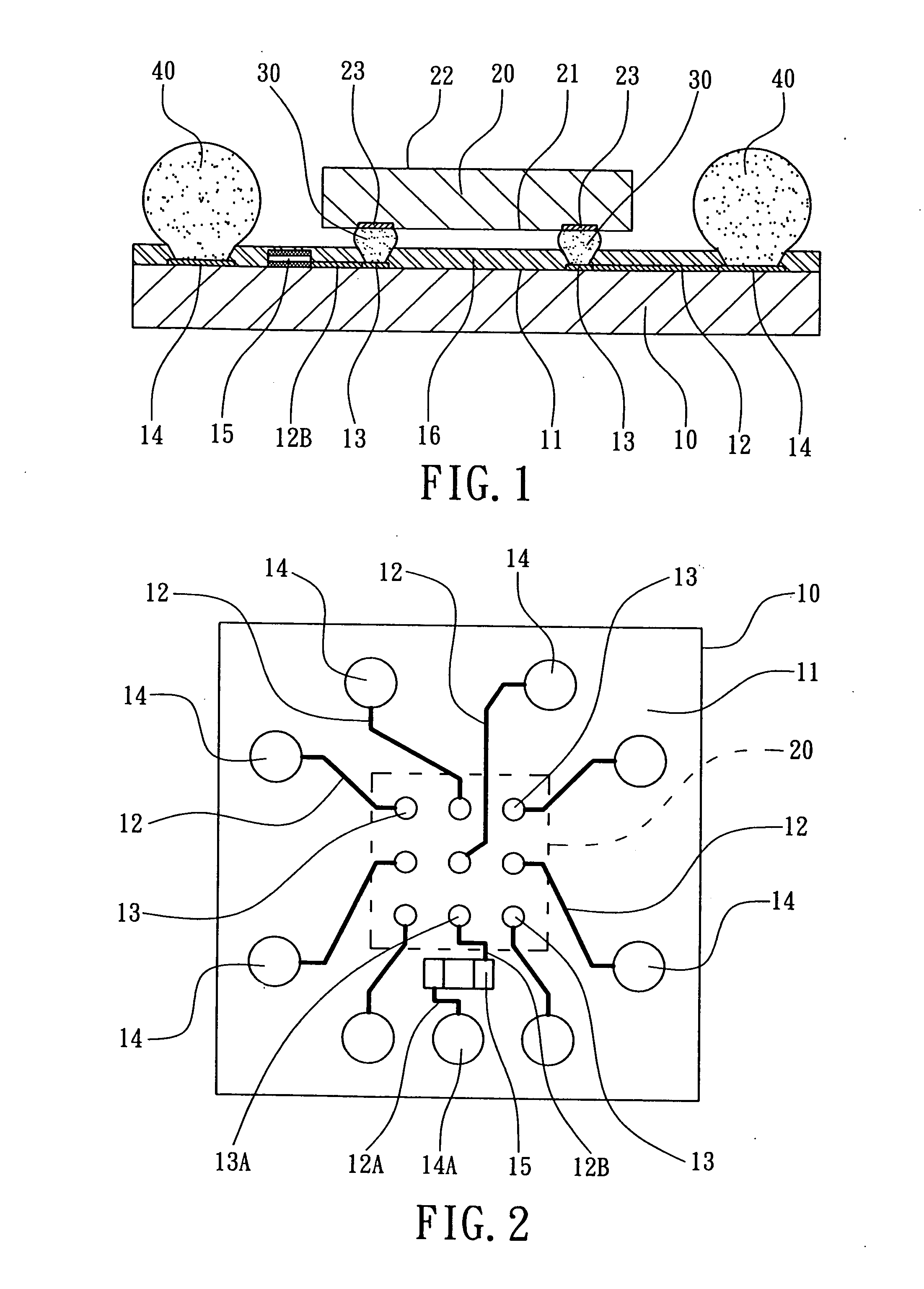
[0004] The main objective of the present invention is to provide an integrated circuit device with embedded passive components by flip-chip connection. The embedded passive component is included in a dummy chip and is electrically connected to a flip chip by flip-chip connection. The dummy chip has a chip-mounting surface and includes a plurality of redistribution traces and a plurality of flip-chip pads. Bumps on the active surface of the flip chip are connected to the flip-chip pads. Accordingly, the embedded passive component in the dummy chip is electrically connected to the flip chip by flip-chip connection. The dummy chip with the embedded passive component and the flip chip with active components can be fabricated by different wafer processes to achieve higher yield and lower fabrication cost.
[0005] The secondary objective of the present invention is to provide an integrated circuit device including a flip chip mounted on a dummy chip. The dummy chip includes an embedded component, such as passive components, optical electronic components or MEMS (micro-electro-mechanical system) components, which is made by a wafer fabrication process different from that of the flip chip. The dummy chip also includes a plurality of redistribution traces and a plurality of flip-chip pads. The embedded component is electrically connected to one of the flip-chip pads via one of the redistribution traces so as to be electrically connected to the flip chip with a short electrical path. Accordingly, the embedded component in the dummy chip can be fabricated separately so as to obtain higher yield, lower fabrication cost with minimum electrical interference.

Problems solved by technology

However since the operative functions of integrated circuit device become complicated and various, SIP (system in package) solution becomes more practicable than SOC.
Since the different material characteristics and manufacturing processes between active components and passive components (ordinarily active components are made by thin film wafer fabrication processes and passive components are made by thick film wafer fabrication processes), it is very difficult to manufacture embedded passive components inside an IC chip.
Especially for the IC chip with RF (radio frequency) functions, the resistance of the embedded passive component in a chip cannot precisely control.
The quality and yield of the IC chip is worse due to the embedded passive component inside the IC chip.
Because the passive component is much cheaper than the IC chip and also is made by different wafer fabrication processes, a passive component embedded in IC chip will result in lower yield and higher fabrication cost.

Method used


Image

  • Integrated circuit device with embedded passive component by flip-chip connection and method for manufacturing the same
  • Integrated circuit device with embedded passive component by flip-chip connection and method for manufacturing the same
  • Integrated circuit device with embedded passive component by flip-chip connection and method for manufacturing the same

Examples


Embodiment Construction

[0008] Referring to the drawings attached, the present invention will be described by means of the embodiment below.

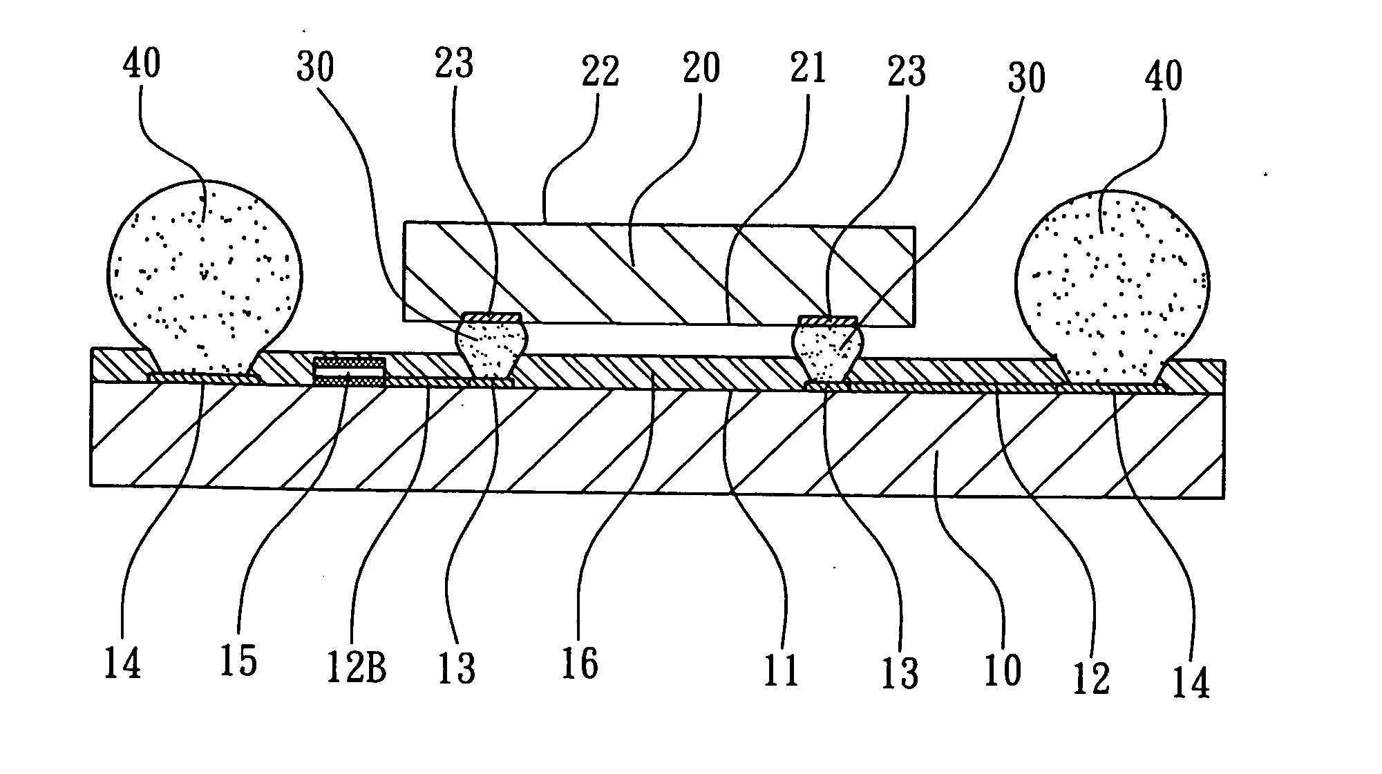
[0009] Referring to FIG. 1, an integrated circuit device with embedded passive component by flip-chip connection is provided in accordance with the present invention. The integrated circuit device generally comprises a dummy chip 10, a flip chip 20 and a plurality of solder balls 40. Referring to FIG. 1 and FIG. 2, the dummy chip 10 has a chip-mounting surface 11. And the dummy chip 10 includes at least an embedded passive component 15, a plurality of redistribution traces 12, a plurality of flip-chip pads 13 and a plurality of ball pads 14. The dummy chip 10 is a semiconductor substrate made of silicon or gallium arsenide. The chip-mounting surface 11 is larger than the active surface 21 of the flip chip 20. The plurality of redistribution traces 12, the flip-chip pads 13 and the ball pads 14 are formed on the chip-mounting surface 11. One ends of the redistribution ...


PUM


Abstract

An integrated circuit device with embedded passive component by flip-chip connection is provided which includes a flip chip and a dummy chip. The dummy chip includes at least an embedded passive component, a plurality of redistribution traces and a plurality of flip-chip pads. The flip chip is smaller than the dummy chip and is mounted on a surface of the dummy chip with the flip-chip pads. The embedded passive component is electrically connected to the flip chip via the redistribution traces and the flip-chip pads. A plurality of solder balls are placed at the peripheral region of the surface of the dummy chip.

Description

FIELD OF THE INVENTION [0001] The present invention relates to an integrated circuit device, more particularly to an integrated circuit device with embedded passive component in a dummy chip. BACKGROUND OF THE INVENTION [0002] The conventional integrated circuit device generally includes active components such as transistors and diodes in a chip, and passive components such as condensers and resistosr, conductive traces in / on a substrate. In SOC (system on chip) technology, all the active components and passive components are intended to be fabricated in high density on the active surface of a chip. However since the operative functions of integrated circuit device become complicated and various, SIP (system in package) solution becomes more practicable than SOC. Since the different material characteristics and manufacturing processes between active components and passive components (ordinarily active components are made by thin film wafer fabrication processes and passive component...

Claims


Application Information

Patent Timeline
IPC IPC(8): H01L25/065H01L25/16
CPCH01L25/0657H01L2924/1461H01L2224/16H01L2225/06513H01L2225/06527H01L2924/15173H01L2924/15311H01L2924/1532H01L2924/19105H01L2924/01019H01L2924/01087H01L2924/13091H01L2224/16237H01L2224/81191H01L25/16H01L2924/00H01L2224/05548H01L2224/05567H01L2224/05571H01L2224/05573H01L2924/00014H01L2224/06131H01L2224/0615H01L2224/02379H01L24/05H01L2224/05599
Inventor TSAI, MON-CHIN
Owner ADVANCED SEMICON ENG INC
Learn More