Organic lights-emitting device with doped emission layer

Active Publication Date: 2005-03-03
SAMSUNG DISPLAY CO LTD
View PDF7 Cites 93 Cited by
  • Summary
  • Abstract
  • Description
  • Claims
  • Application Information

AI Technical Summary

Benefits of technology

[0009] The present invention provides an OLED having enhanced luminous efficienc

Problems solved by technology

However, in this case, a concentration quenching phenomena may occur to thereby reduce the luminous efficiency.
However, forming the blocking layer as a common layer on the red

Method used


Image

  • Organic lights-emitting device with doped emission layer
  • Organic lights-emitting device with doped emission layer
  • Organic lights-emitting device with doped emission layer

Examples


first example

Ir(ppy)3 10 wt. %-7 wt. %-4 wt. % graded EML

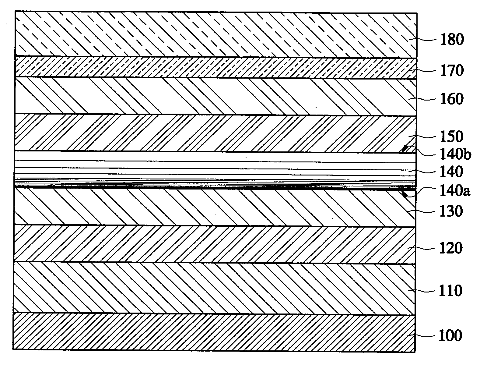
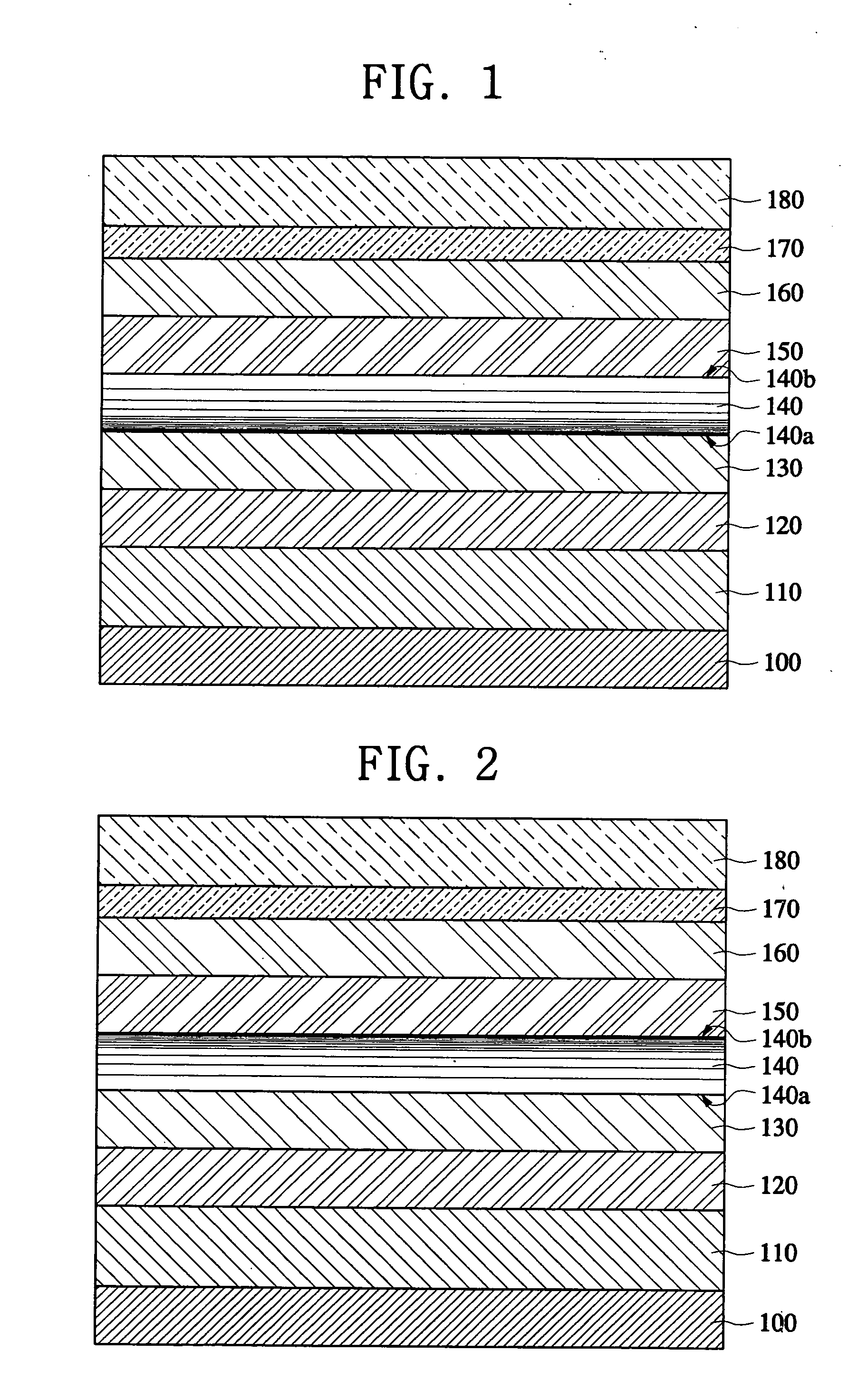
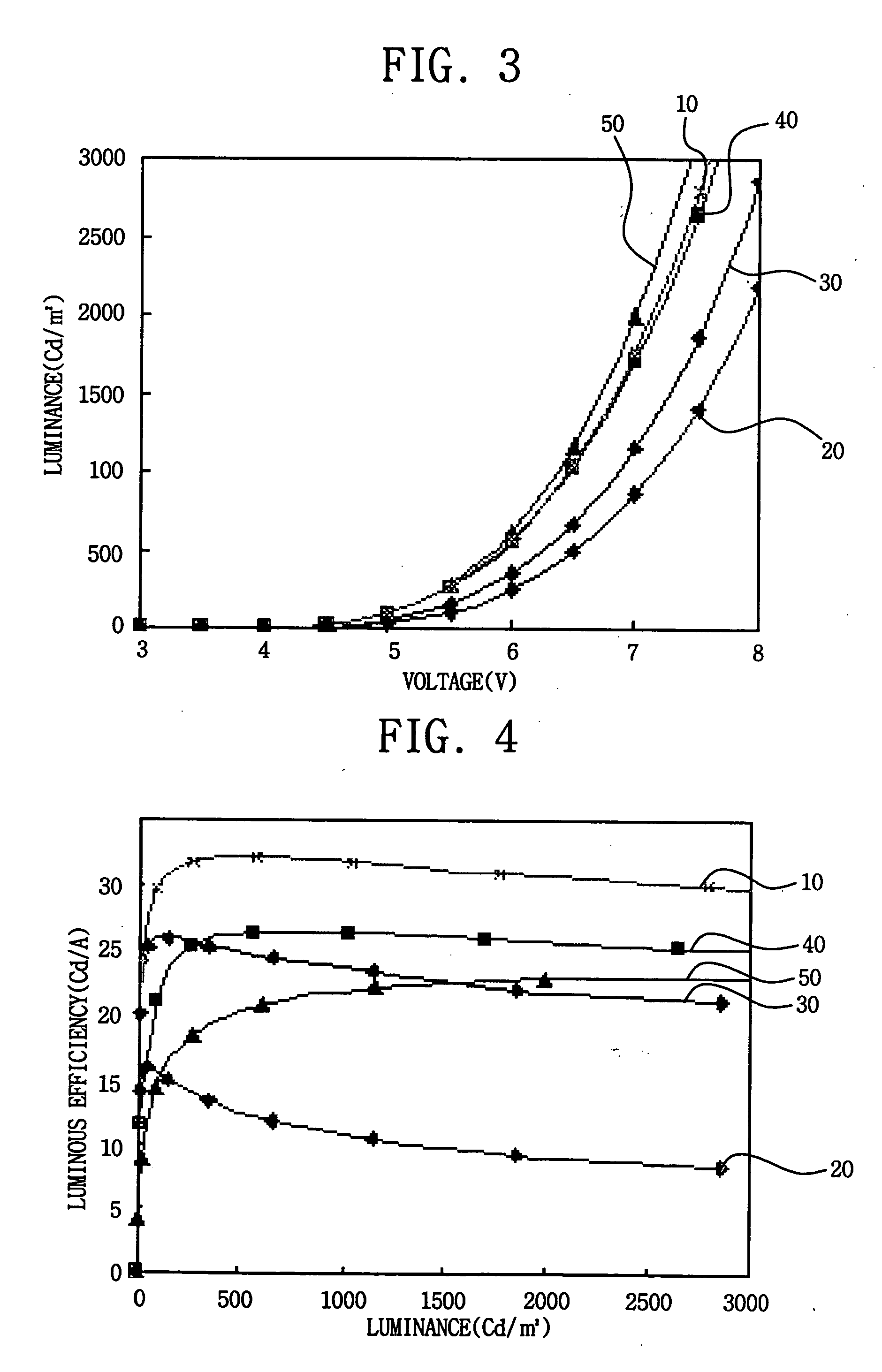
[0035] An ITO substrate patterned with a width of 80 μm was subject to an ultrasonic cleaning and UV-O3 treatment, and a small-molecule type material of IDEMITZ 406 (available from IDEMITZ Co. and with a 5.1 eV of HOMO (Highest Occupied Molecular Orbital)) was then vacuum deposited with a thickness of 600 Å to form an HIL. A non-polymer material of IDEMITZ 320 (available from IDEMITZ Co. and with a 5.4 eV of HOMO) was then vacuum deposited with a thickness of 300 Å to form a HTL. A host material of CBP and Ir(ppy)3 was codeposited with a thickness of 80 Å on the HTL so as to have the concentration of Ir(ppy)3, which is a green phosphorus dopant, be 10% by weight, and CBP and Ir(ppy)3 was codeposited with a thickness of 80 Å so as to have the concentration of Ir(ppy)3 be 7% by weight, and CBP and Ir(ppy)3 was codeposited with a thickness of 80 Å so as to have the concentration of Ir(ppy)3 be 4% by weight, so that the EML having a total thi...

second example

RD61 4%-8%-12% graded EML

[0043] An ITO substrate patterned with a width of 80 μm was subject to an ultrasonic cleaning and UV-O3 treatment, and non-polymer material of IDEMITZ 406 (available from IDEMITZ Co. and with a HOMO of 5.1 eV) was vacuum deposited with a thickness of 600 Å to form an HIL. A non-polymer material of IDEMITZ 320 (available from IDEMITZ Co. and with a 5.4 eV of HOMO) was then vacuum deposited with a thickness of 300 Å to form an HTL. A host material of CBP and RD61 (Iridium (III)bis(1-phenyl(quinolinato-N,C2′))acetylacetonate, available from UDC Co.) was codeposited with a thickness of 100 Å on the HTL so as to have the concentration of RD61, which is a red phosphorus dopant, be 4% by weight, and CBP and RD61 was codeposited with a thickness of 100 Å so as to have the concentration of RD61 be 8% by weight. CBP and RD61 was codeposited with a thickness of 100 Å so as to have the concentration of RD61 be 12% by weight, so that a EML having a total thickness of 30...


PUM

PropertyMeasurementUnit
Percent by massaaaaaaaaaa
Thicknessaaaaaaaaaa

Abstract

An OLED has a doped emission layer (EML). The OLED comprises a first electrode, a second electrode, and an EML having a host material and a light-emitting dopant and interposed between the first electrode and the second electrode, wherein the light-emitting dopant has a concentration gradient between a first surface close to the first electrode of the EML and a second surface opposite to the first surface. As a result, luminous efficiency of the OLED can be enhanced and a driving voltage can also be reduced.

Description

CROSS-REFERENCE TO RELATED APPLICATION [0001] This application claims the benefit of Korea Patent Application No. 2003-61591 filed on Sep. 3, 2003, the disclosure of which is incorporated herein by reference in its entirety. FIELD OF THE INVENTION [0002] The present invention relates to an organic light-emitting device (hereinafter, referred to as OLED) and, more particularly, to an OLED with a doped emission layer. BACKGROUND OF THE INVENTION [0003] In general, an OLED is an emissive device and has been highlighted as the next generation display because it not only has a wide viewing angle and a good contrast but also a fast response time. [0004] The OLED comprises an anode, a cathode and an emission layer (hereinafter, referred to as EML) interposed between the anode and the cathode. When a voltage is applied between the anode and the cathode, holes and electrons are injected into the EML, and then combined in the EML to create exitons, which decay radiatively. This radiation is c...

Claims


Application Information

Patent Timeline
IPC IPC(8): H01J1/62H01L51/00H01L51/50H05B33/14H05B33/00
CPCH01L51/0062H01L51/0085H01L2251/5346H01L51/5016H01L51/5012H10K85/649H10K85/342H10K50/11H10K2101/10H10K2101/80H10K10/00H05B33/14
Inventor CHIN, BYUNG-DOOSUH, MIN-CHULKIM, MU-HYUNYANG, NAM-CHOULLEE, SEONG-TAEK
Owner SAMSUNG DISPLAY CO LTD
Why Eureka
Try Eureka