Active sensor and method for optical illumination and detection

a technology of active sensors and detection methods, applied in the field of optical measurement systems, can solve the problems of poor spatial resolution of ccd-based approaches, long scanning time and moving parts, lack of sensitivity, etc., and achieve the effects of high sensitivity, low cost and high speed

Inactive Publication Date: 2005-03-03
CROMWELL EVAN FRANCIS +1
View PDF5 Cites 38 Cited by
  • Summary
  • Abstract
  • Description
  • Claims
  • Application Information

AI Technical Summary

Benefits of technology

[0010] The above objectives of providing a method and system for performing active one-dimensional and two-dimensional optical measurements having high speed, high sensitivity and low cost is accomplished in a meth

Problems solved by technology

The disadvantages of the above-described systems and methods are long scanning times and moving parts for the SCM-based approach and lack of sensitivity and poorer spatial resolution for the CCD-based approach.
A third alternative has been implemented, using a scanning laser and a photomultiplier tube for detection, but t

Method used


Image

  • Active sensor and method for optical illumination and detection
  • Active sensor and method for optical illumination and detection
  • Active sensor and method for optical illumination and detection

Examples


Embodiment Construction

[0020] While the below description is limited, by the way of example, to the measurement of a fluorescent sample, it is understood that the function will be similar for samples such as colored materials, MEMS or semiconductor devices, and / or repetitive patterns, and other applications. In order to avoid repetition, it is understood that the same description will be applicable to other applications that measure optical properties of samples.

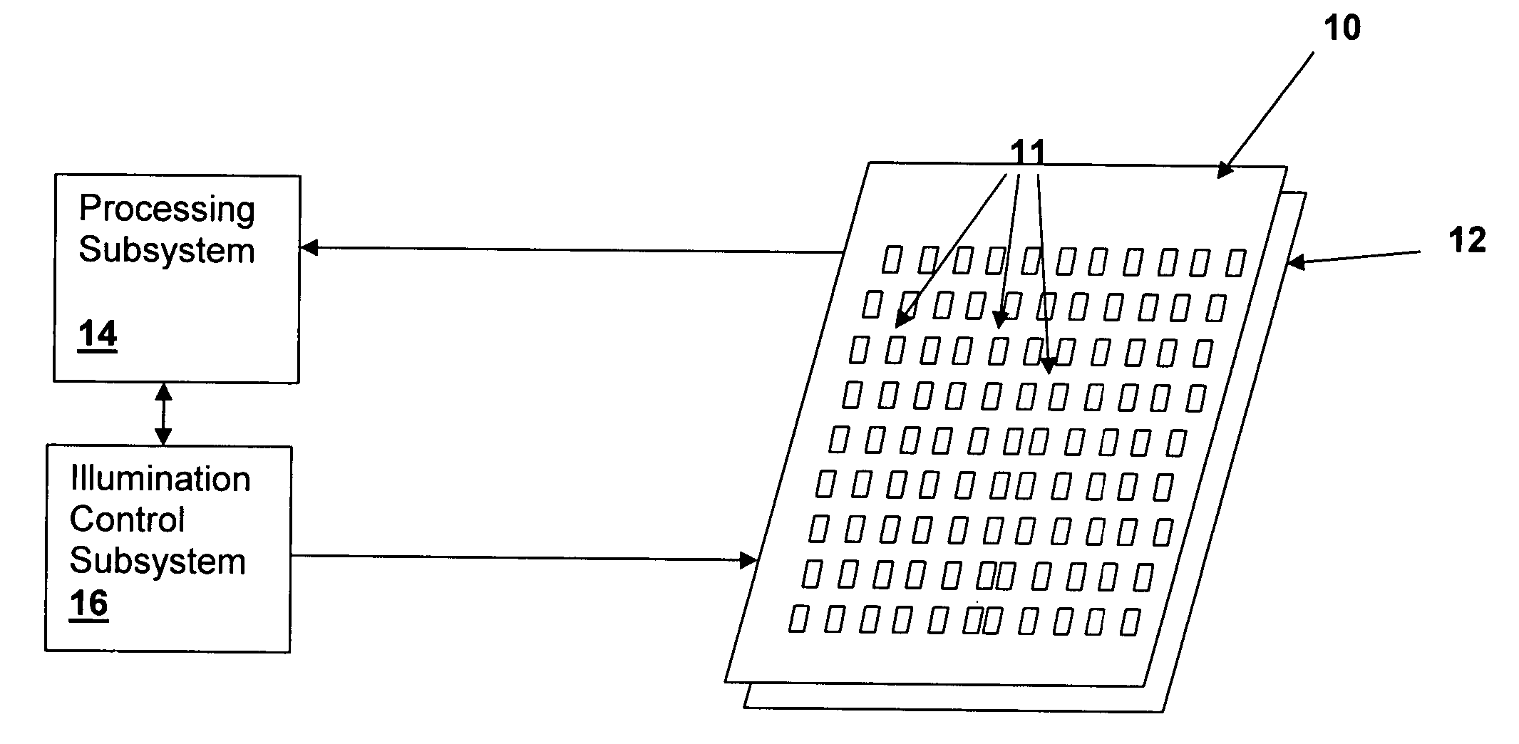
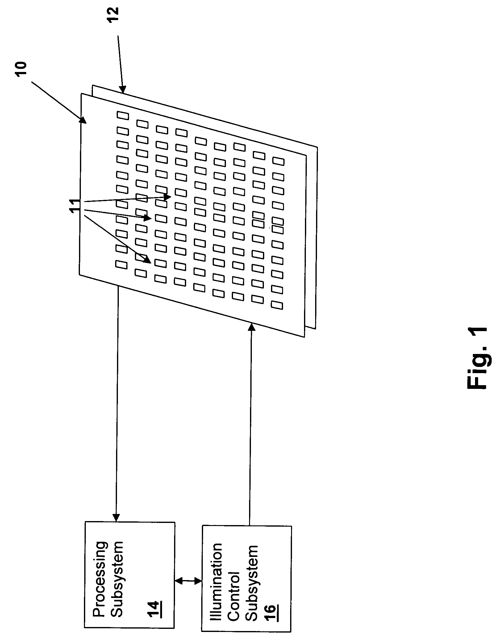
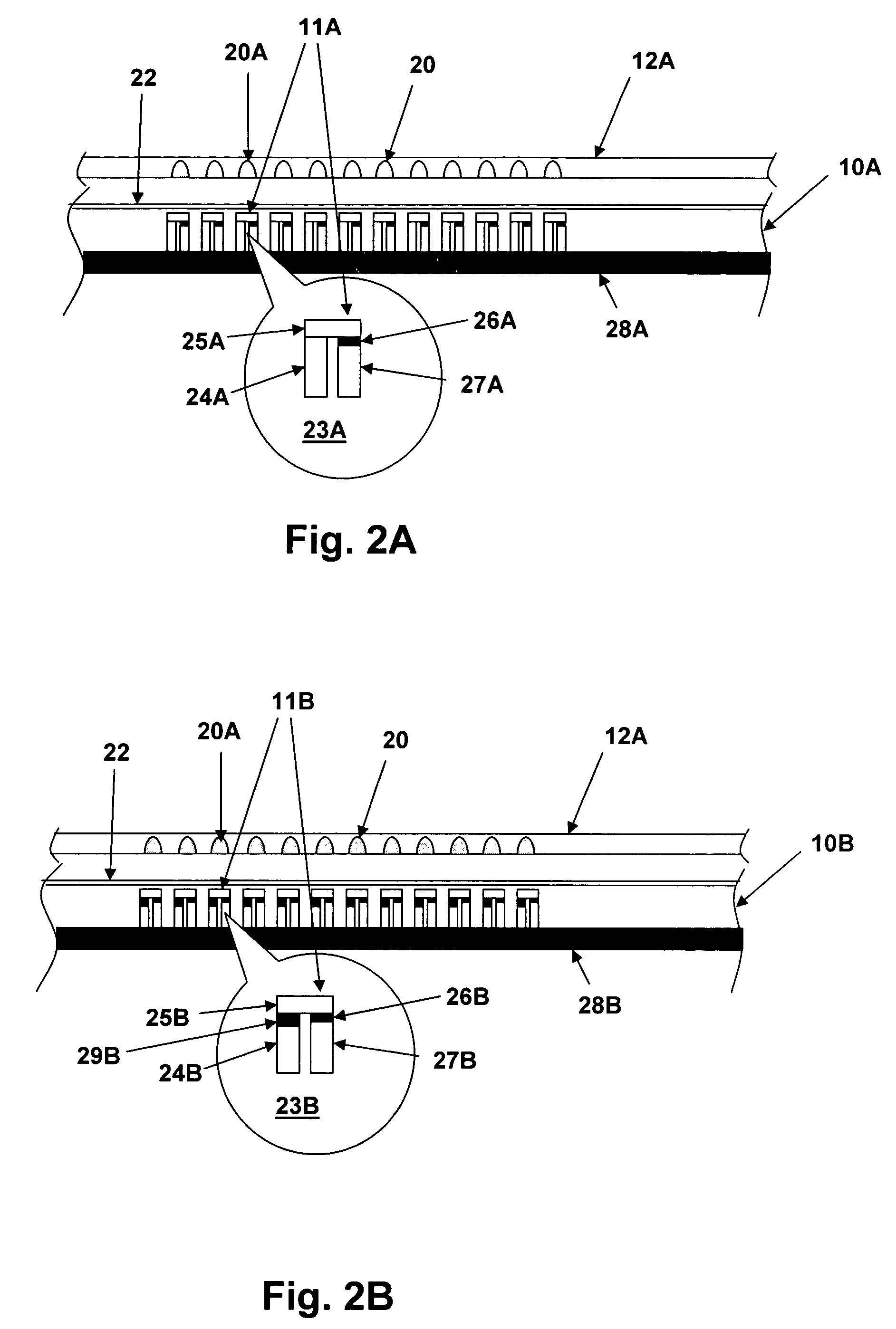
[0021] Referring now to the figures and in particular to FIG. 1, a system including an active sensor 10 in accordance with an embodiment of the present invention is shown. Active sensor 10, which includes a plurality of active sensor active sensor cells 11, is placed in close proximity with a sample frame 12, that may contain samples of biological matter tagged with a fluorescent material, or other samples under inspection such as a semiconductor device, for which a standard handling frame may be employed. Active sensor cells 11 each include one ...


PUM


Abstract

An active sensor a method for optical illumination and detection provides low cost and high-speed optical scanning of bio-arrays, DNA samples/chips, semiconductors, micro-electromechanical systems and other samples requiring inspection or measurement. A plurality of illumination sources forming a parallel multi-pixel array is used to illuminate one or more samples via an imaging system or by placement in close proximity to the samples. The array may be a line array or a two-dimensional array. A plurality of detectors is integrated within the multi-pixel illumination array or provided in a separate array, each detector for detecting optical properties of the sample that results from illumination by one or more associated illumination sources. One detector may be associated with multiple illuminators or one illuminator may be associated with multiple detectors. Filters may be integrated within the illumination path and/or detection paths to provide wavelength and/or polarization discrimination capability and microlenses may also be incorporated within the illumination path and/or detection paths to provide focusing or imaging. The illumination sources may be provided by TFT-LCD devices, diode emitters, organic LEDs (OLEDs), vertical cavity emitting lasers (VCELs) or other light sources that may be integrated to form a high-density illumination matrix. The detectors may be PIN photo-diodes or other suitable detectors that are capable of integration within the illumination matrix.

Description

BACKGROUND OF THE INVENTION [0001] 1. Field of the Invention [0002] The present invention relates generally to optical measurement systems, and more specifically, to an active sensor illumination and detection apparatus for performing sample measurements using associated detector / illuminator groups integrated on one or more substrates. [0003] 2. Background of the Invention [0004] One-dimensional and two dimensional measurement and inspection of samples is commonly performed in many industries, including biotechnology, semiconductor, micro electro-mechanical systems (MEMS) and others. For example, in the biotechnology industry, fluorescence measurements are used to determine the response of biological matter to illumination, thus revealing information about the composition and structure of a sample. Typically, for biological fluorescence tests, a sample or a material that is introduced to a sample is “tagged” with a fluorescent compound, the sample is illuminated with a laser, and th...

Claims


Application Information

Patent Timeline
IPC IPC(8): B01L3/00G01N21/64
CPCB01J2219/00693B01J2219/00702G01N21/6454B01L2300/0654B01L2300/0829B01L3/5085
Inventor CROMWELL, EVAN FRANCISBRUNFELD, ANDREI
Owner CROMWELL EVAN FRANCIS
Why Eureka
Try Eureka