

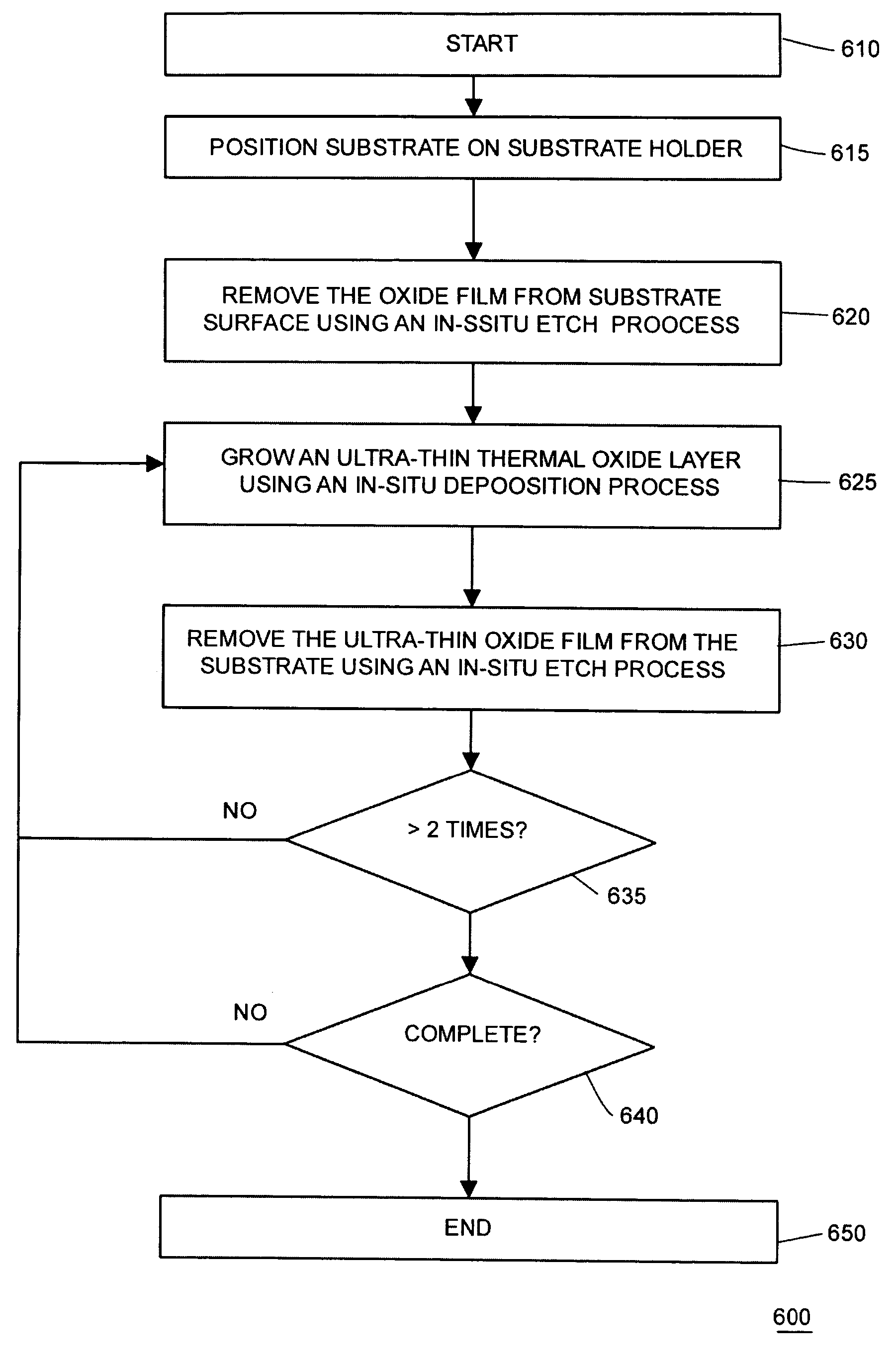
Multiple grow-etch cyclic surface treatment for substrate preparation
- Summary
- Abstract
- Description
- Claims
- Application Information
AI Technical Summary
Benefits of technology
Problems solved by technology
Method used
Image

Examples
Embodiment Construction
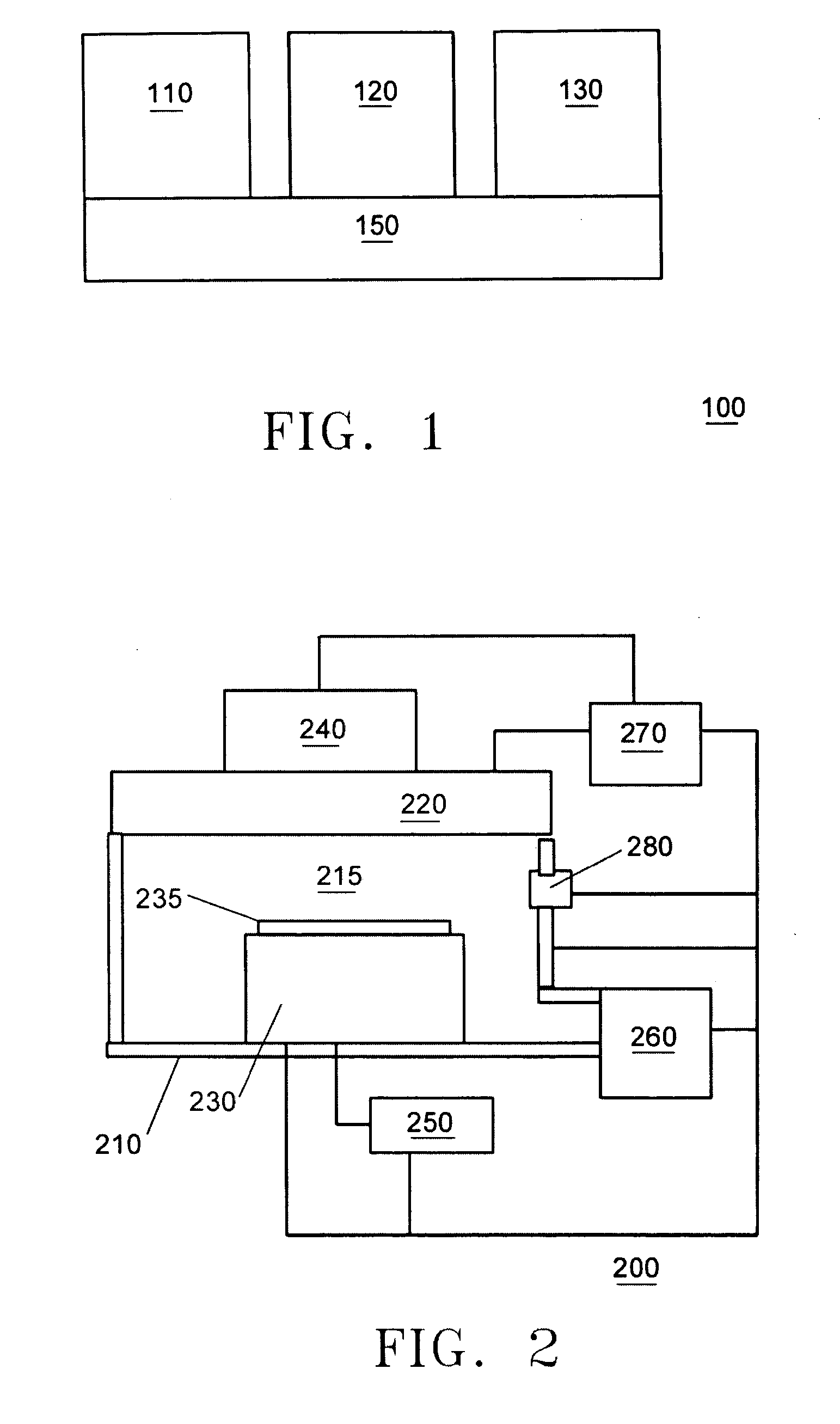
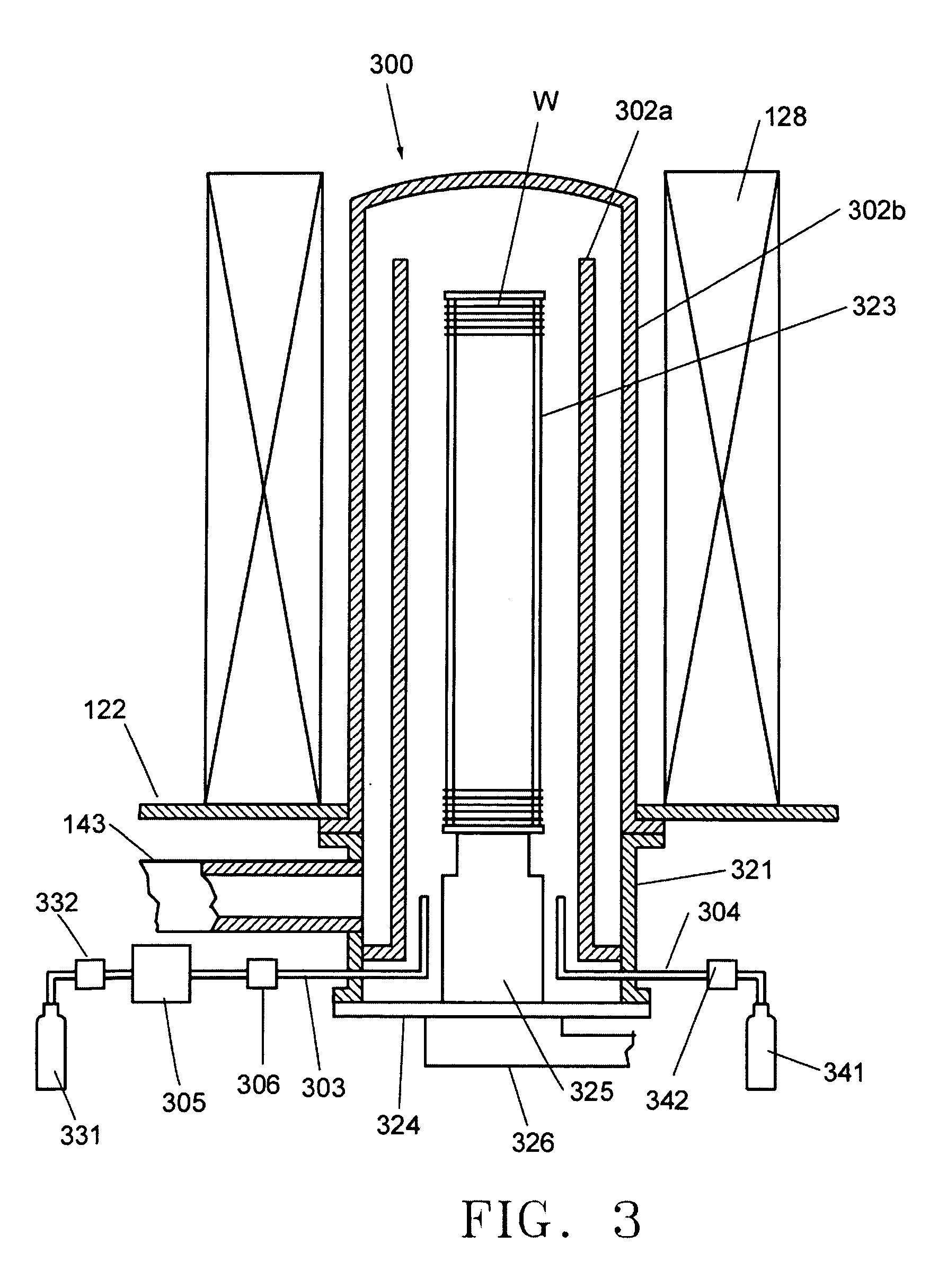
[0019] Referring now to the drawings, FIG. 1 shows an exemplary block diagram of a processing system in accordance with one embodiment of the present invention. Processing system 100 includes a number of processing modules 110-130 coupled to a transfer system 150 and may be used to perform the processing steps of the present invention, including those described with respect to FIGS. 5A-5G below, for example. Although three processing modules are shown in FIG. 1, any number of processing modules can be used. For example, process modules can include a dry etching process module, a wet etching process module, a thermal oxidation process module, a spin-on-glass (SOG) process module, a spin-on-dielectric (SOD) process module for measuring substrate parameters including internal and external properties, a chemical vapor deposition (CVD) process module, a physical vapor deposition (PVD) process module, an ionized physical vapor deposition (iPVD) process module, an atomic layer deposition (...
PUM
 Abstract
Description
Claims
Application Information