Display device and method for manufacturing the same

a technology for display devices and manufacturing methods, applied in static indicating devices, semiconductor/solid-state device details, instruments, etc., can solve the problems of high resistance of transparent conductive films, low power consumption of display devices disturbed, high resistance of electrodes, etc., to reduce the resistance of electrodes and wiring, reduce power consumption, and reduce the effect of wiring

Inactive Publication Date: 2005-03-10
SEMICON ENERGY LAB CO LTD
View PDF34 Cites 108 Cited by
  • Summary
  • Abstract
  • Description
  • Claims
  • Application Information

AI Technical Summary

Benefits of technology

[0021] The invention is not limited to the provision of the auxiliary wiring for the display device comprising a light-emitting element. The auxiliary wiring may be provided also for a display layer comprising a liquid crystal element, and the resistance of an electrode and a wiring may be reduced.
[0022] According to the auxiliary wiring of the invention, the substantial resistance of an electrode typified by the second electrode, and a wiring can be reduced. The substantial resistance refers to combined resistance of an electrode or a wiring. As a result, reduction in power consumption and prevention of voltage drop due to an electrode and a wiring in the display device can be obtained.
[0023] In addition, a signal writing defect, a gradation defect, and the like due to wiring resistance can be prevented. Furthermore, in the case of the second electrode, the generation of voltage drop can be controlled by connecting it to the auxiliary wiring, so that it is possible to apply uniform amount of voltage to the light-emitting element. Consequently, the improvement of the display quality can be obtained.
[0024] Especially in a large display device, an advantageous effect of reducing substantial resistance of an electrode or a wiring is remarkable.

Problems solved by technology

However, the resistance of the transparent conductive film is high.
As a result, it is concerned that low power consumption of the display device is disturbed.
However, as mentioned above, resistance of the second electrode is high, and consequently it is concerned that power consumption of a display device is increased.

Method used


Image

  • Display device and method for manufacturing the same
  • Display device and method for manufacturing the same
  • Display device and method for manufacturing the same

Examples


embodiment

[0039] (Embodiment Mode 1)

[0040] In this embodiment mode, a configuration of a pixel portion of a display device comprising an auxiliary wiring is described.

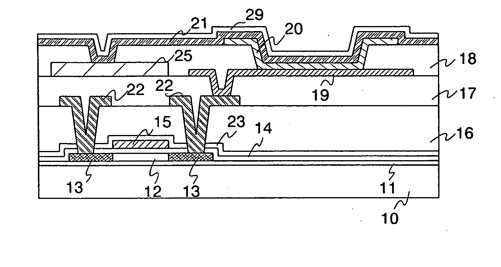
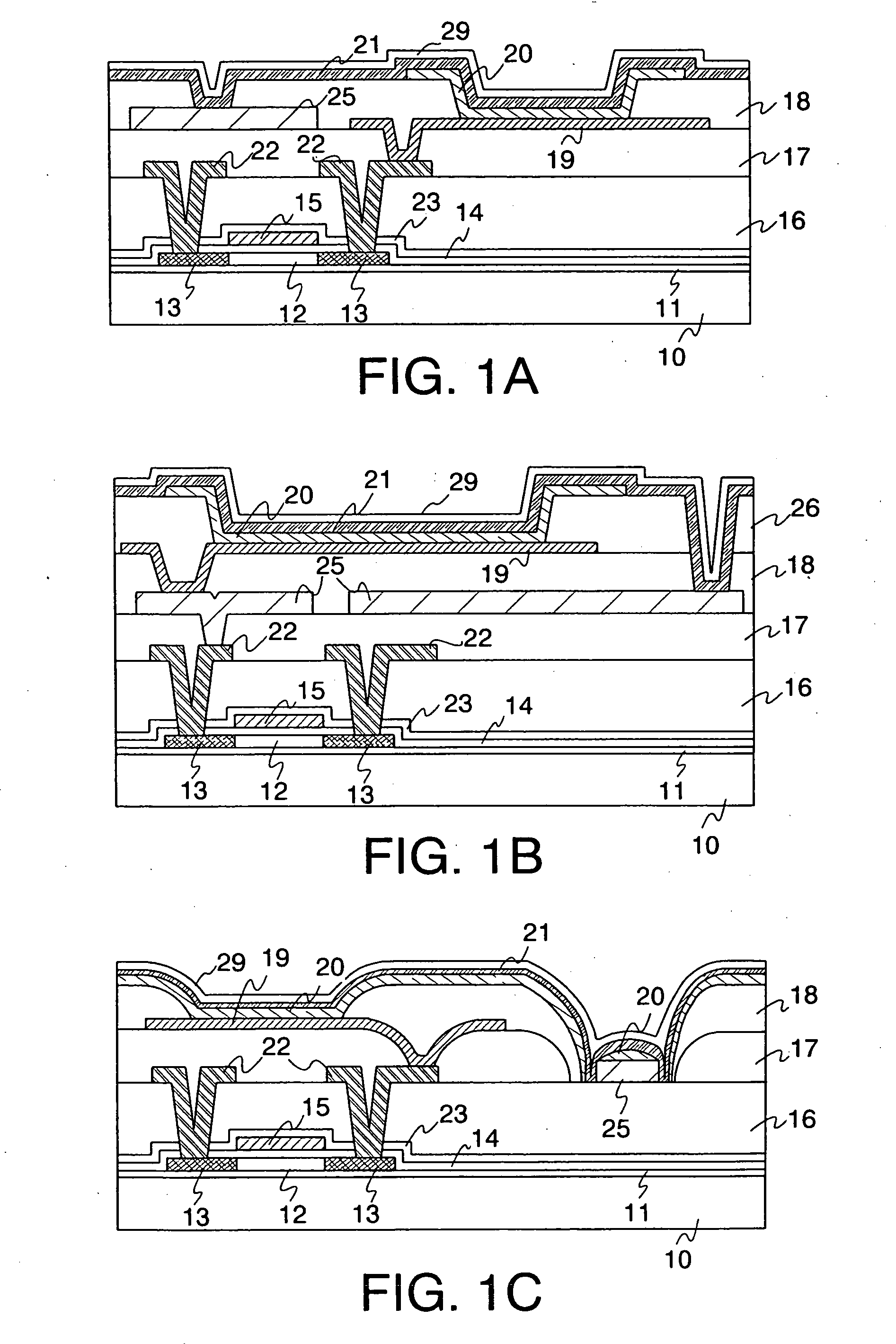
[0041] Configurations are shown in FIGS. 1A to 1C. That is, the configuration of a p-channel type TFT using polycrystalline silicon (polycrystalline TFT) as an example of a semiconductor element, and a pixel portion of the display device in which a transparent conductive film is employed as an example of the second electrode and in which the transparent conductive film that is a second electrode is connected to the auxiliary wiring.

[0042] In FIG. 1A, a configuration in which the second electrode is connected to the auxiliary wiring, and in which the auxiliary wiring is formed in one layer in which a first electrode is formed is shown. Note that the auxiliary wiring may be formed of either the same material as the first electrode or a different material.

[0043] The pixel portion of the display device comprises a base insulating...


PUM


Abstract

An object of the present invention is to decrease substantial resistance of an electrode such as a transparent electrode or a wiring, and furthermore, to provide a display device for which is possible to apply same voltage to light-emitting elements. In the invention, a auxiliary wiring that is formed in one layer in which a conductive film of a semiconductor element such as an electrode, wiring, a signal line, a scanning line, or a power supply line is connected to an electrode typified by a second electrode, and a wiring. It is preferable that the auxiliary wiring is formed into a conductive film to include low resistive material, especially, formed to include lower resistive material than the resistance of an electrode and a wiring that is required to reduce the resistance.

Description

BACKGROUND OF THE INVENTION [0001] 1. Field of the Invention [0002] The present invention relates to a display device equipped with a light-emitting element and a method for manufacturing the same. [0003] 2. Description of the Related Art [0004] In recent years, a large-sized screen and high-definition are promoted in a display device having a light-emitting element and a liquid crystal element, which the number of wirings such as a signal line and a scanning line, and the length of a wiring tend to increase. Therefore, it is necessary to prevent voltage drop due to wiring resistance, a signal writing defect, a gradation defect, and the like. [0005] Thus, there is a configuration in which an auxiliary wiring made of a transparent conductive film is connected to the transparent electrode that the light-emitting element has, interposing an anisotropical conductor (refer to Patent Document 1). According to Patent Document 1, effective resistance of the transparent electrode can be lowe...

Claims


Application Information

Patent Timeline
Patent Type & Authority Applications(United States)
IPC IPC(8): G09G3/32H01L27/32H01L29/04H01L51/52
CPCG09G3/3233G09G2300/0842G09G2300/0861G02F1/133345H01L51/5206H01L51/5221H01L2251/5315H01L27/3276H10K59/131H10K50/81H10K50/824H10K50/828H10K2102/3026H10K50/82H10K50/814H10K59/1315H01L23/5228H01L27/1222H01L27/124H01L27/1248H01L33/40
Inventor MIYAGI, NORIKOSAKAKURA, MASAYUKIARAO, TATSUYANAGAO, RITSUKOTANADA, YOSHIFUMI
Owner SEMICON ENERGY LAB CO LTD
Why Eureka
Try Eureka