Flat panel backlight and liquid crystal display device using the same

a liquid crystal display device and flat panel technology, applied in the field of backlights, can solve the problems of increasing the density of electron linear sources, increasing manufacturing costs, and difficult to increase uniformity, so as to achieve effective improvement of contrast, increase power consumption, and reduce the effect of image quality degradation

Inactive Publication Date: 2005-03-10
HITACHI DISPLAYS
View PDF9 Cites 11 Cited by
  • Summary
  • Abstract
  • Description
  • Claims
  • Application Information

AI Technical Summary

Benefits of technology

[0015] As has been explained heretofore, according to the present invention, by adopting a flat panel light emitting element, which uses field emission electron sources that are capable of performing line-scanning-type monochroic light emission, as a backlight which illuminates a liquid crystal panel part, it is possible to obtain a flat panel backlight which is capable of obtaining an image display with the least degradation of image quality, such as blurring on the moving image, in particular. Further, by setting the light emission strength of the flat panel backlight at a high brightness partially and for a short time so as to properly control the optical transmissivity of the liquid crystal element, it is possible to effectively improve the contrast with only a slight increase of the power consumption, and, hence, it is possible to provide a liquid crystal display device which is capable of producing a high quality display.

Problems solved by technology

However, in the structure disclosed in patent literature 1, since it is necessary to arrange a plurality of linear electron sources at given positions in a distributed manner, the density of the electron linear sources is increased, whereby it is difficult to increase the uniformity, thus increasing the manufacturing cost.
Further, the light emission state of a phosphor screen is uniform over the whole screen, and, hence, to avoid degradation of the image quality when a moving image is displayed, that is, to prevent moving image blurring, the method of driving the liquid crystal element becomes complicated.
Further, to construct a structure which allows for selective emission of lights of plural colors, as disclosed in patent literature 2, it is necessary to strictly align the loci of electron beams which constitute an excitation source of the phosphors with the arrangement of the phosphors and, further, with the arrangement of pixels of the liquid crystal element; and, hence, a restriction is imposed on the setting of the strength of the electron beams, or the manufacturing cost is increased due to this alignment.
Because of the necessity for alignment, the necessity of providing a panel structure which enables high-speed driving and the necessity of providing a drive device which can cope with the high-speed driving, the manufacturing cost is increased.

Method used


Image

  • Flat panel backlight and liquid crystal display device using the same
  • Flat panel backlight and liquid crystal display device using the same
  • Flat panel backlight and liquid crystal display device using the same

Examples


Embodiment Construction

[0027] Preferred embodiments of the display device of the present invention will be explained in detail hereinafter in conjunction with the drawings.

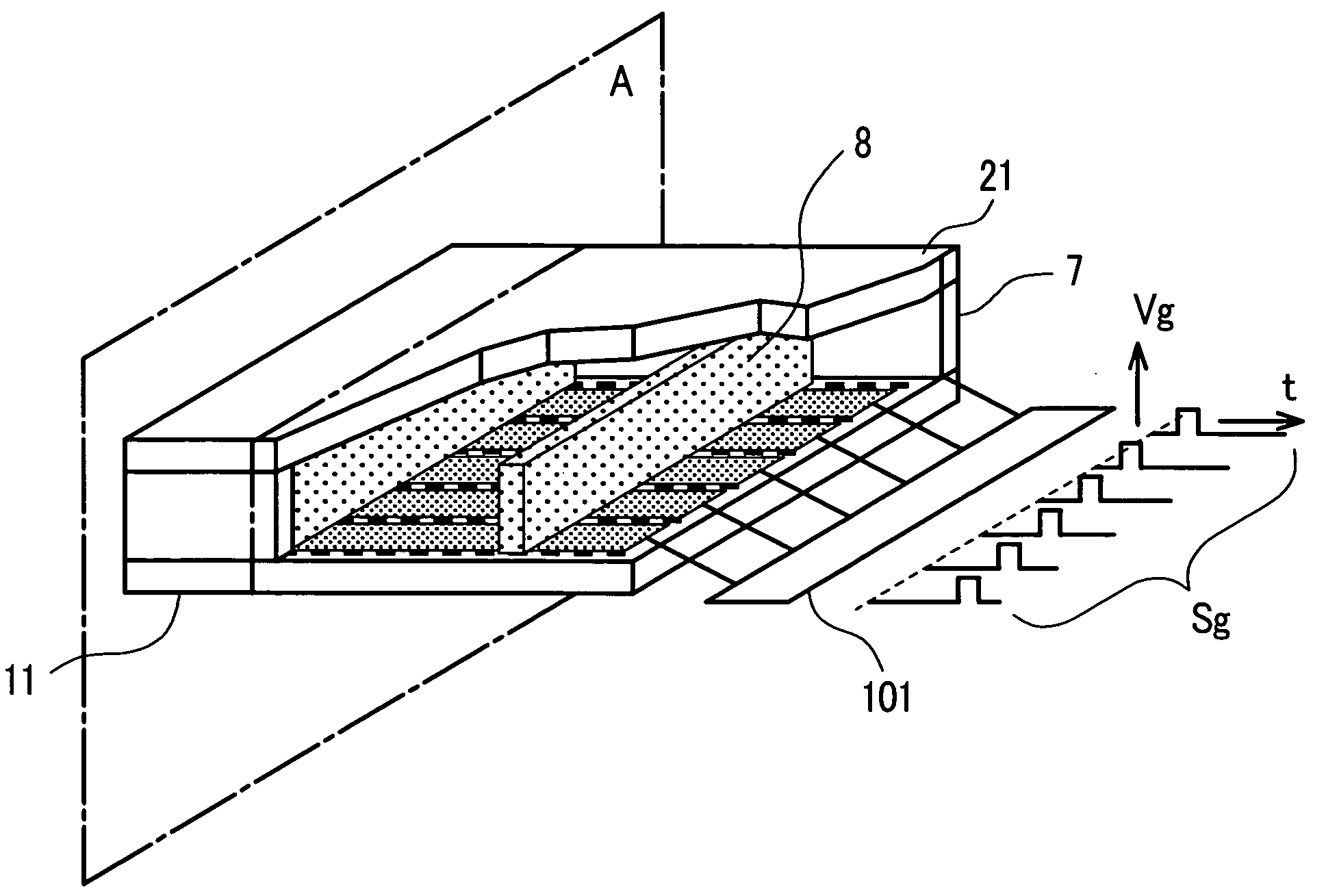
[0028]FIG. 1 is a perspective view showing the constitution of a first embodiment of a flat panel backlight according to the present invention.

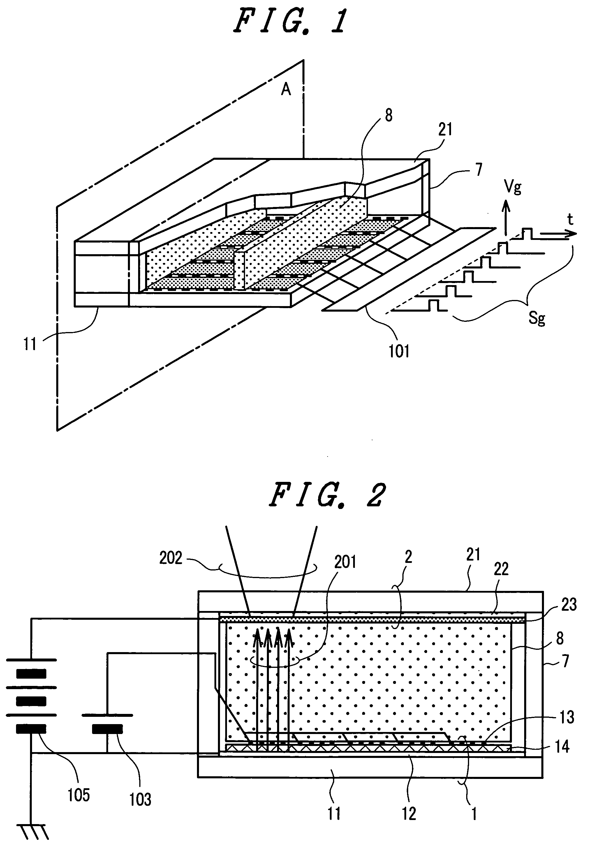
[0029] Further, FIG. 2 is a cross-sectional view taken along a plane A in FIG. 1. The flat panel backlight of this embodiment is of a type in which a light emitting region is divided by a plurality of control electrodes. Here, FIG. 2 shows the constitution of the electrodes and the voltage applied state.

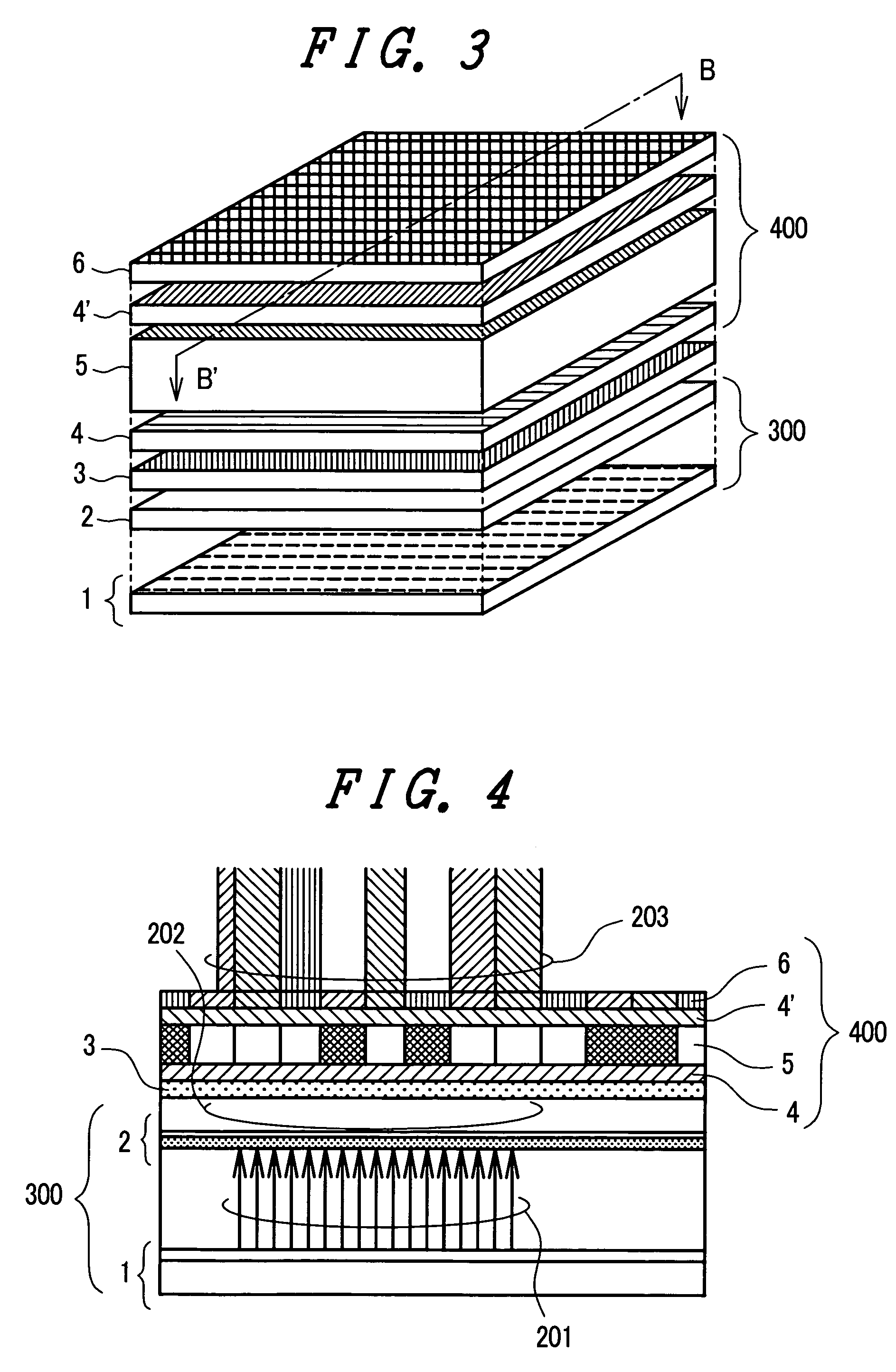
[0030] In this embodiment, to ensure the required conductivity in a region which corresponds to the light emitting region on an electron beam source panel glass substrate 11, a silver paste is printed and baked to form a background having a thickness of 5 μm. Thereafter, a paste containing 10% by weight of carbon fibers, mainly formed of the carbon nanotubes having a length of 5 μm, is printed ...


PUM

PropertyMeasurementUnit
thicknessaaaaaaaaaa
lengthaaaaaaaaaa
widthaaaaaaaaaa

Abstract

To obtain an image display of high image quality with a high and contrast with the least blurring, an electron beam source panel includes cathodes which emit electron beams and control electrodes which control the strength of the electron beams, and a phosphor screen panel includes a light emitting surface having a phosphor capable of emitting light of the same color over the whole light emitting surface and anodes to which a potential is supplied necessary for the phosphor. The electron beam source panel and the phosphor screen panel are laminated to each other by way of spacers, the laminated structure is sealed by a frame glass and the inside of the sealed structure is evacuated to create a vacuum therein. The light emitting surface is divided in three or more regions, thus providing a flat panel backlight which selectively allows only some portions of the divided light emitting surface to emit light.

Description

BACKGROUND OF THE INVENTION [0001] The present invention relates to a backlight of the type used in combination with a liquid crystal element; and, more particularly, the invention relates to a flat panel backlight forming a field emission light emitting element which uses a cold cathode material which generates an electron emission in a relatively low electric field, particularly to a carbon-oriented material, such as carbon nanotubes, fine carbon fibers, diamond or the like, without being heated to a high temperature, and the invention relates further to a liquid crystal display device which combines the flat panel backlight and a liquid crystal element. [0002] A thin light source, which utilizes the emission of light obtained by the radiation of electron beams emitted from a cathode (a linear cathode) to a phosphor, in the same manner as a cathode ray tube, as a backlight of a liquid crystal display device, is described in Japanese Unexamined Patent Publication Sho63(1988)-10458 ...

Claims


Application Information

Patent Timeline
Patent Type & Authority Applications(United States)
IPC IPC(8): G02F1/13357F21S2/00G02F1/133H01J1/62H01J63/04H01J63/06
CPCH01J63/06G02F2001/133622G02F1/133622
Inventor YAGUCHI, TOMIOHAYASHI, NOBUAKIOKAI, MAKOTOMUNEYOSHI, TAKAHIKO
Owner HITACHI DISPLAYS
Why Eureka
Try Eureka