Semiconductor integrated circuit in which voltage down converter output can be observed as digital value and voltage down converter output voltage is adjustable

a technology of integrated circuits and semiconductors, applied in logic circuit coupling/interface arrangements, pulse techniques, instruments, etc., can solve the problems of low current supply capability of booster circuits embedded in non-volatile memory, generated high voltage is not resistant to noise, generated high voltage cannot be output to an external terminal, etc., to reduce the number of man-hours, facilitate mass production testing, and reduce the effect of design evaluation

Inactive Publication Date: 2005-03-10
RENESAS TECH CORP
View PDF14 Cites 13 Cited by
  • Summary
  • Abstract
  • Description
  • Claims
  • Application Information

AI Technical Summary

Benefits of technology

[0010] An object of the present invention is to provide a semiconductor integrated circuit allowing for efficient design evaluation, facilitated mass production test, and reduction in the number of man-hours in the mass production test by utilizing functions of an integrated circuit for testing of another integrated circuit in a semiconductor integrated circuit implemented by integrating a voltage down converter, an A / D converter and other logic circuits. In addition, it is also an object of the present invention to suppress the number of input / output terminals in the semiconductor integrated circuit.
[0011] More specifically, the present invention aims to observe a voltage associated with the voltage down converter as a digital value by utilizing a function of the A / D converter as well as to determine the voltage associated with the voltage down converter or to control the same so as to obtain an appropriate voltage. In this manner, the present invention aims to reduce the number of terminals for observing the voltage directly associated with the voltage down converter.
[0013] Therefore, the present invention is primarily advantageous in that an internal voltage is output as a digital signal by utilizing the A / D converter integrated on a chip, which will for allow facilitated measurement and reduction in the number of test terminals for voltage monitoring.

Problems solved by technology

Current supply capability of a booster circuit embedded in a non-volatile memory is extremely low, and a generated high voltage is not resistant to noise or the like.
As such, the generated high voltage cannot be output to an external terminal.
On the other hand, integration on a chip of an A / D converter dedicated for a test in order to check an internally generated voltage leads to an increase in a chip area, which is not advantageous in terms of cost.
Recently, a circuit size of a semiconductor integrated circuit has increased as the development of system-on-chip, and accordingly, an increase in the number of man-hours in a mass production shipment test as well as in design verification has been an issue.
Therefore, a measurement system has been complicated.
In addition, circuit size of the individual circuit has increased, which leads to an increase in the number of man-hours in mass production test and design evaluation.
Moreover, the number of input / output terminals of these semiconductor integrated circuits has increased, and an area for arranging input / output pads is not negligible, considering the chip size of the semiconductor integrated circuit.

Method used


Image

  • Semiconductor integrated circuit in which voltage down converter output can be observed as digital value and voltage down converter output voltage is adjustable
  • Semiconductor integrated circuit in which voltage down converter output can be observed as digital value and voltage down converter output voltage is adjustable
  • Semiconductor integrated circuit in which voltage down converter output can be observed as digital value and voltage down converter output voltage is adjustable

Examples


embodiment 1

[0040] [Embodiment 1]

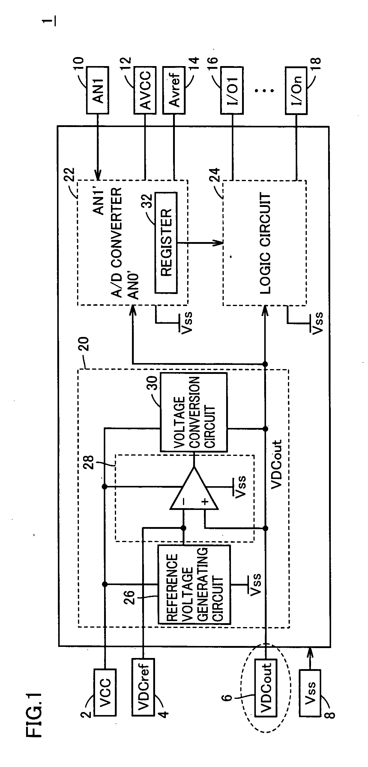
[0041]FIG. 1 is a block diagram showing a configuration of a semiconductor integrated circuit 1 in Embodiment 1 of the present invention.

[0042] Referring to FIG. 1, semiconductor integrated circuit 1 includes terminals 2, 4, 6, 8, 10, 12, 14, and 16 to 18, a voltage down conversion (VDC) circuit 20, an A / D converter 22, and a logic circuit 24.

[0043] VDC circuit 20 includes a reference voltage generating circuit 26, a differential amplifier 28, and a voltage conversion circuit 30. A / D converter 22 includes a register 32 storing a result of A / D conversion.

[0044] A power supply voltage VCC is supplied for VDC circuit 20 from terminal 2. A power supply voltage AVCC is supplied for A / D converter 22 via terminal 12. A voltage VDCout which is an output of VDC circuit 20 is supplied to logic circuit 24. In other words, respective circuits operate by receiving separate power supply voltages. Here, a ground voltage VSS, that is, ground, is common to each circuit for th...

embodiment 2

[0050] [Embodiment 2]

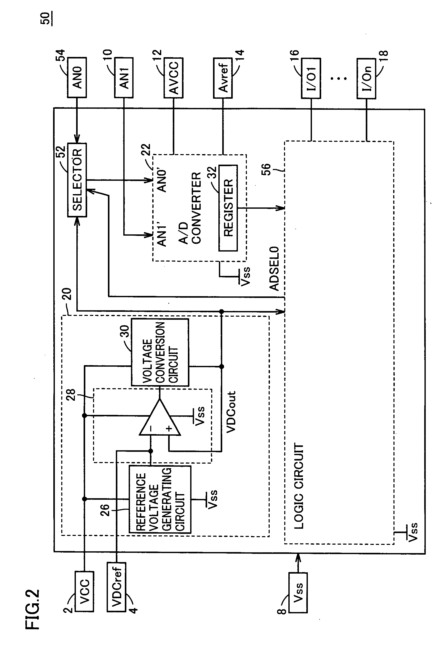
[0051]FIG. 2 is a block diagram showing a configuration of a semiconductor integrated circuit 50 in Embodiment 2.

[0052] Referring to FIG. 2, semiconductor integrated circuit 50 in Embodiment 2 includes a logic circuit 56 instead of logic circuit 24 in the configuration of semiconductor integrated circuit 1 shown in FIG. 1, and further includes a terminal 54 and a selector 52.

[0053] Logic circuit 56 outputs a signal ADSEL0 for selecting an input to the A / D converter. Terminal 54 is provided for input of an analog input signal AN0. Selector 52 selects signal AN0 or voltage VDCout output by VDC circuit 20 in accordance with signal ADSEL0, and provides the selected one to input node AN0′ of A / D converter 22.

[0054] Embodiment 2 is characterized by selector 52 including two inputs and having an output connected to analog input node AN0′ of A / D converter 22.

[0055] In Embodiment 1, analog input node AN0′ of A / D converter 22 has been coupled to output voltage VDCout ...

embodiment 3

[0061] [Embodiment 3]

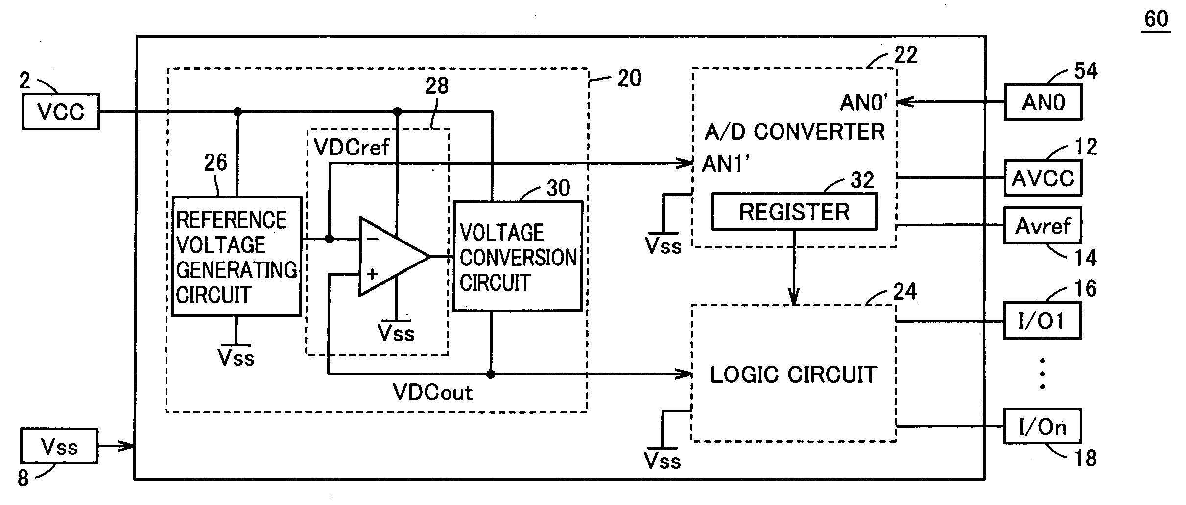
[0062]FIG. 3 is a block diagram showing a configuration of a semiconductor integrated circuit 60 in Embodiment 3.

[0063] Referring to FIG. 3, semiconductor integrated circuit 60 includes terminal 54 for providing analog signal AN0, whereas terminals 4, 6 and 10 are eliminated from the configuration of semiconductor integrated circuit 1 shown in FIG. 1. A / D converter 22 receives analog signal AN0 provided to input node AN0′ via terminal 54, and receives reference voltage VDCref output by reference voltage generating circuit 26 at an input node AN1′. The configuration is otherwise the same as that shown in FIG. 1, and description thereof will not be repeated.

[0064] VDC circuit 20 inputs output voltage VDCout of VDC circuit 20 and reference voltage VDCref which is the output voltage of reference voltage generating circuit 26 to differential amplifier 28. Differential amplifier 28 controls voltage conversion circuit 30 in accordance with a difference between these ...


PUM


Abstract

An output voltage of a VDC circuit is subjected to A / D conversion with an on-chip A / D converter. Accordingly, an output voltage VDCout of the VDC circuit can be observed as a digital value, which facilitates measurement. Reduction in the number of terminals leads to reduction in chip size. In addition, the terminal that has been used for providing voltage VDCout can be used for other purposes. Therefore, a semiconductor integrated circuit allowing for easy mass production test and reduced number of man-hours in the mass production test can be provided.

Description

BACKGROUND OF THE INVENTION [0001] 1. Field of the Invention [0002] The present invention relates to a semiconductor integrated circuit. [0003] 2. Description of the Background Art [0004] Current supply capability of a booster circuit embedded in a non-volatile memory is extremely low, and a generated high voltage is not resistant to noise or the like. As such, the generated high voltage cannot be output to an external terminal. In such a situation, Japanese Patent Laying-Open No. 5-325580 discloses a technology to check an internal voltage by embedding an A / D (analog / digital) converter for a test, dividing the generated high voltage for conversion by the A / D converter so as to output a resultant digital signal to the outside, and monitoring the digital signal. [0005] On the other hand, integration on a chip of an A / D converter dedicated for a test in order to check an internally generated voltage leads to an increase in a chip area, which is not advantageous in terms of cost. [0006...

Claims


Application Information

Patent Timeline
Patent Type & Authority Applications(United States)
IPC IPC(8): G01R31/316G01R31/28G11C5/14G11C16/00G11C16/06G11C16/26G11C29/00G11C29/02H01L21/822H01L27/04H03K19/00H03K19/0175H03M1/12
CPCG11C29/02G11C2029/5004G11C29/028G11C29/021G11C16/00G11C16/06G11C16/26
Inventor NAKANO, TADAYOSHINASU, TAKASHI
Owner RENESAS TECH CORP
Why Eureka
Try Eureka