Optical device and methods of manufacture

a technology of optical variable devices and optical components, applied in the field of optical devices, can solve the problems of counterfeiting problems, high cost of these technologies, and added problems and potential security risks, and achieve the effects of improving the quality of optical components, and improving the accuracy of optical components

Inactive Publication Date: 2005-03-10
CCL SECURE PTY LTD
View PDF7 Cites 20 Cited by
  • Summary
  • Abstract
  • Description
  • Claims
  • Application Information

AI Technical Summary

Benefits of technology

According to an aspect of the present invention, a more general and useful approach to the design of optically reflecting or diffracting microstructures is obtained by utilising colour component values (such as the red, green and blue values) of each pixel in the optically invariable image and relating these parameters via a mathematical or computer algorithm to the parameters required to define the geometrical surface shape properties of each small surface region of the three dimensional reflective or diffractive microstructure.

Problems solved by technology

In spite of their industrial effectiveness these foil based diffractive optically variable devices also represent relatively expensive solutions to the counterfeiting problem when compared to the more traditional security printing technologies such as watermarking and intaglio printing.
The expensive nature of these technologies is due to the requirement for embossing the diffractive microstructure into a metallized plastic foil prior to the application of this foil onto the valuable document
Because the embossing of the OVD microstructure takes place in a specialised foil production facility external to the security printing works there is also the added problem and potential security risk if the high security foil supplies are lost or stolen in transit to the security printing plant.
However the variability of the surface profile of the device, and therefore the consequent optical variability of any image generated by the device, is limited by the requirement of having only one pixel parameter (the greytone value) in the optically invariable image relate to the geometrical characteristics of the three dimensional microstructure.
In particular this one parameter limitation means that only the height of the microstructure is able to be controlled within each small region of the microstructure.
Therefore both the geometrical surface characteristics and the method of manufacture of the device described in PCT / AU99 / 00741 are of limited utility in terms of industrial application.

Method used


Image

  • Optical device and methods of manufacture
  • Optical device and methods of manufacture
  • Optical device and methods of manufacture

Examples


Embodiment Construction

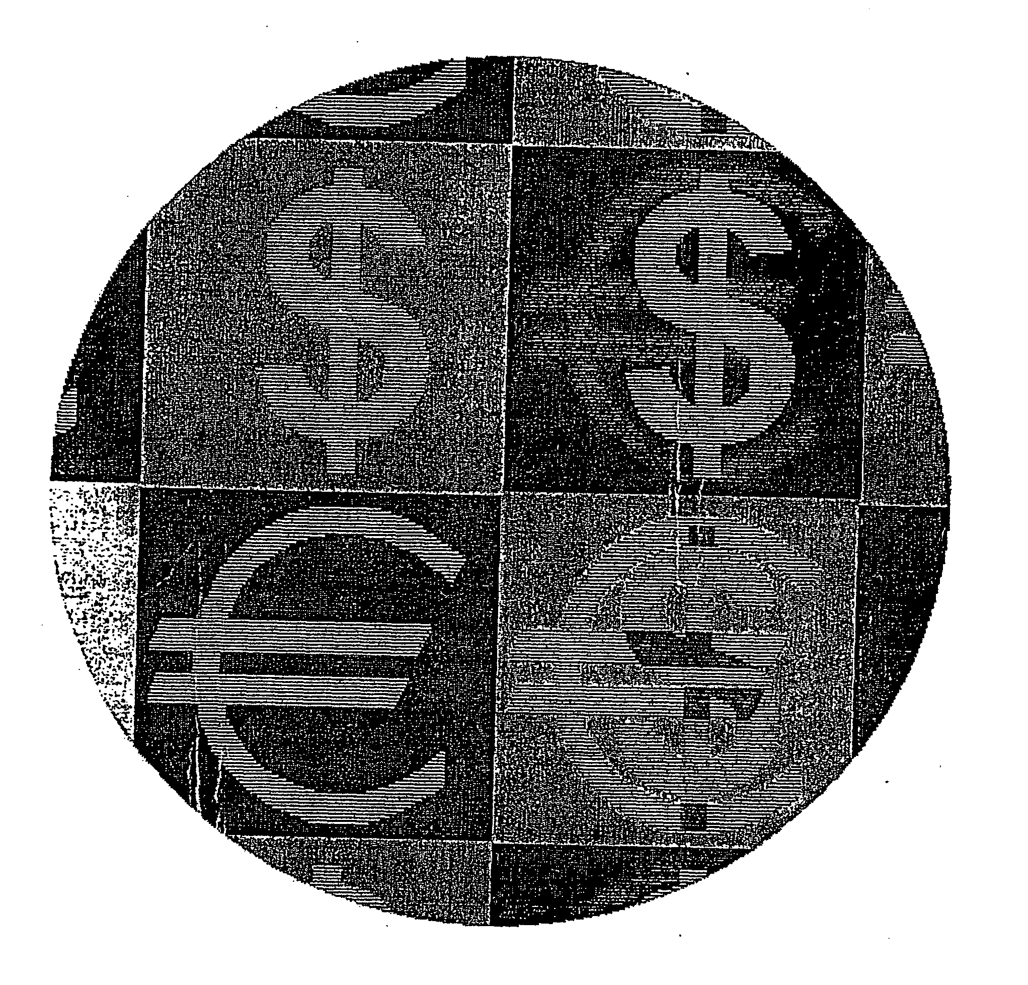
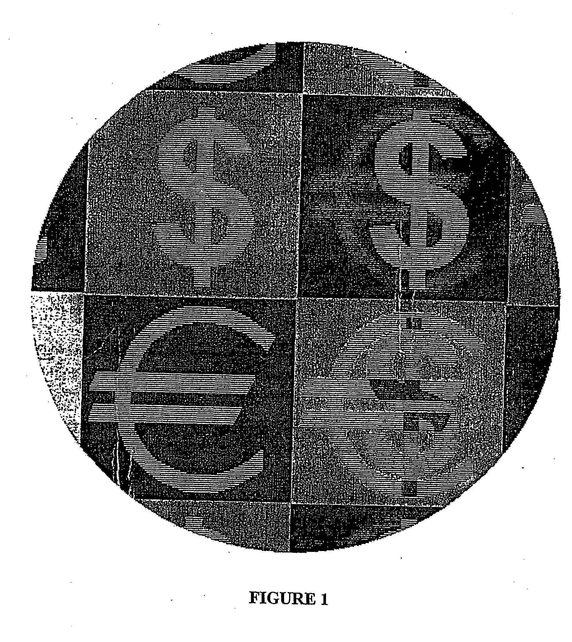
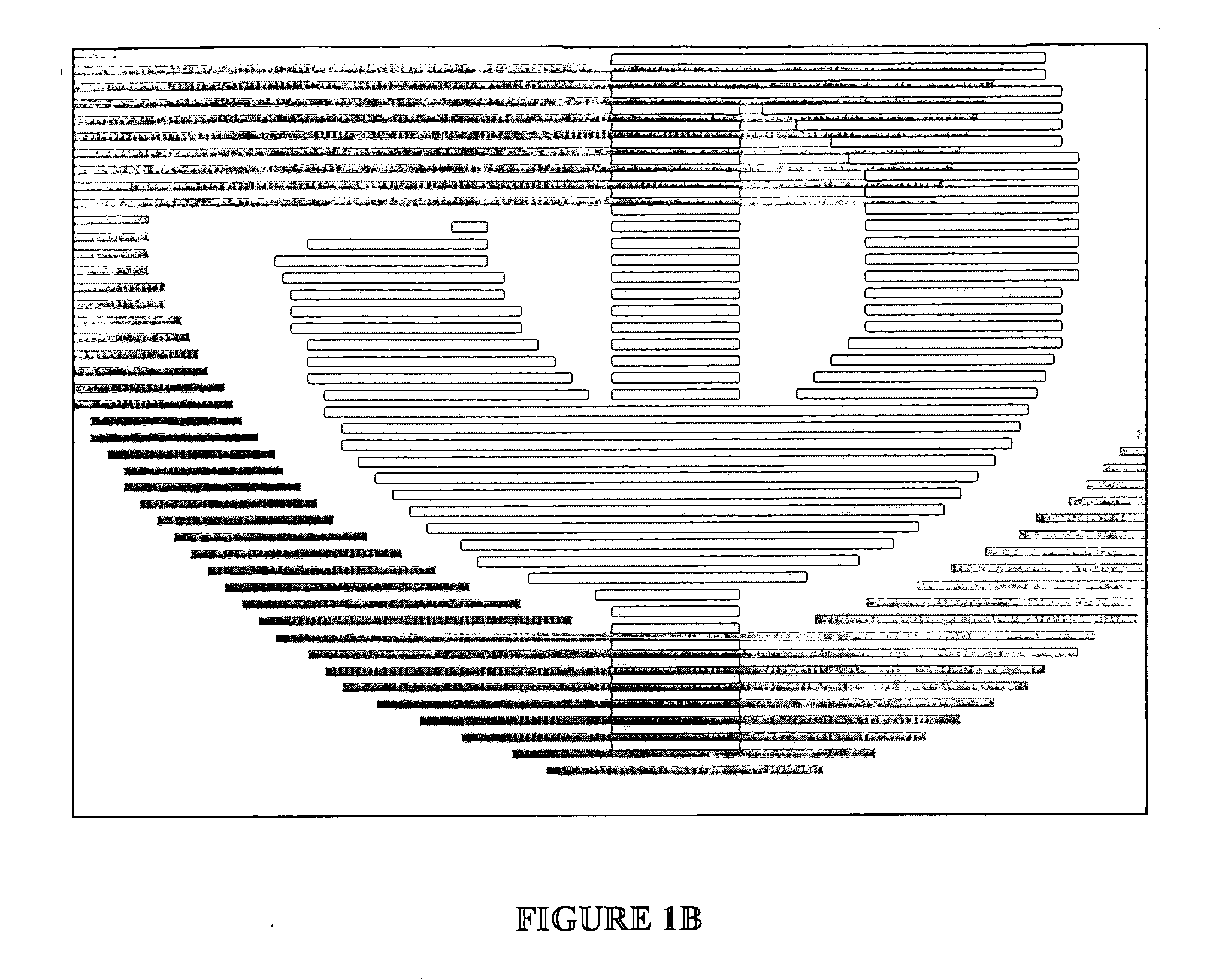
The present invention relates to high security Optically Variable Device (OVD) microstructures and generalised reflecting or diffracting surface structures, particularly for non foil based applications where direct printing into the application substrate or direct reflection or diffraction from the replicated surface structure of the device is a specific requirement. Unlike foil based diffractive microstructures which require the microstructure to be embossed into a hot stamping foil prior to application onto the document substrate, these new specialised microstructure geometries have a particular application related to direct printing onto the document via the use of specialised inks and lacquers. In order to avoid problems associated with the thickness variations in the paper surface (e.g. due to paper fibre variations) the microstructure of the OVD incorporates surface relief variations of relatively large depth dimension (eg 15 to 100 microns).

Specific microstructures of inte...


PUM


Abstract

An optical device which generates an optically variable image, the image being optically variable in that it varies according to the position of observation, is manufactured by dividing an optically invariable image into multiple pixels. Colour component values are determined for each pixel. For each of the pixels of the optically invariable image, there is determined an associated pixel surface structure which has a three-dimensional surface shape and curvature which is related via a mathematical of computer algorithm to the oclour component values of the associated pixel in the optically invariable image, each pixel surface structure being an individual reflective or diffractive surface structure which produces an observable optical effect. An assembly of the reflective or diffractive pixel surface structures is produced which when illuminated generates a plurality of observable optical effects wihch combine to form an optically variable reproduction of the optically invariable image.

Description

FIELD OF THE INVENTION This invention relates to an optical device, and in particular to an optical device which, when illuminated by a light source generates one or more images which are observable from particular ranges of viewing angles around the device. The device may be used in a number of different applications, and it has particular application as an anti-forgery security device on banknotes, credit cards, cheques, share certificates and other valuable documents. BACKGROUND ART The new series of American Express US dollar travellers cheques, first issued in 1997, employs as an anti-counterfeiting feature a diffraction grating foil image of the American Express Centurion logo. When illuminated by a light source and the diffraction grating foil device is observed from different viewing angles the Centurion image appears to switch to an American Express box logo image. This optical variability of the device ensures that it is impossible to copy by normal photocopier or camera...

Claims


Application Information

Patent Timeline
Patent Type & Authority Applications(United States)
IPC IPC(8): B41M3/06B41M3/14B42D25/00B42D25/29B42D25/328B44F1/10G02B5/18
CPCB41M3/06B41M3/148B44F1/10B42D25/328G03H2224/02B42D25/29B42D25/00G02B5/1861B42D25/41B42D25/425B42D25/324B42D25/47B42D25/44B42D25/445B42D25/373G03C8/56
Inventor LEE, ROBERT ARTHUR
Owner CCL SECURE PTY LTD
Why Eureka
Try Eureka