Integrated circuit card and a method of manufacturing the same

a manufacturing method and integrated circuit technology, applied in the field of integrated circuit card manufacturing, can solve the problems of increasing the size of the chip incorporated in the card or a multi-chip structure, the inside diameter of the cavity cannot be expanded to near the card size (15 mm25 mm), and the function of the portable telephone can be easily extended. , the effect of simplifying the assembly process

Inactive Publication Date: 2005-03-10
RENESAS ELECTRONICS CORP
View PDF12 Cites 16 Cited by
  • Summary
  • Abstract
  • Description
  • Claims
  • Application Information

AI Technical Summary

Benefits of technology

[0031] By constructing the body of the plug-in UICC with use of a molding resin, it is possible to increase the size of each chip and the number of chips to be mounted on the card, so that the function of the portable telephone can

Problems solved by technology

However, for extending the function of the portable telephone, an increase in the size of the chip incorporated in the card or a multi-chip structure is required.
As to the existing plug-in SIM cards having the above-mentioned structure, however, studies made by the present in

Method used


Image

  • Integrated circuit card and a method of manufacturing the same
  • Integrated circuit card and a method of manufacturing the same
  • Integrated circuit card and a method of manufacturing the same

Examples


first embodiment

[0057] (First Embodiment)

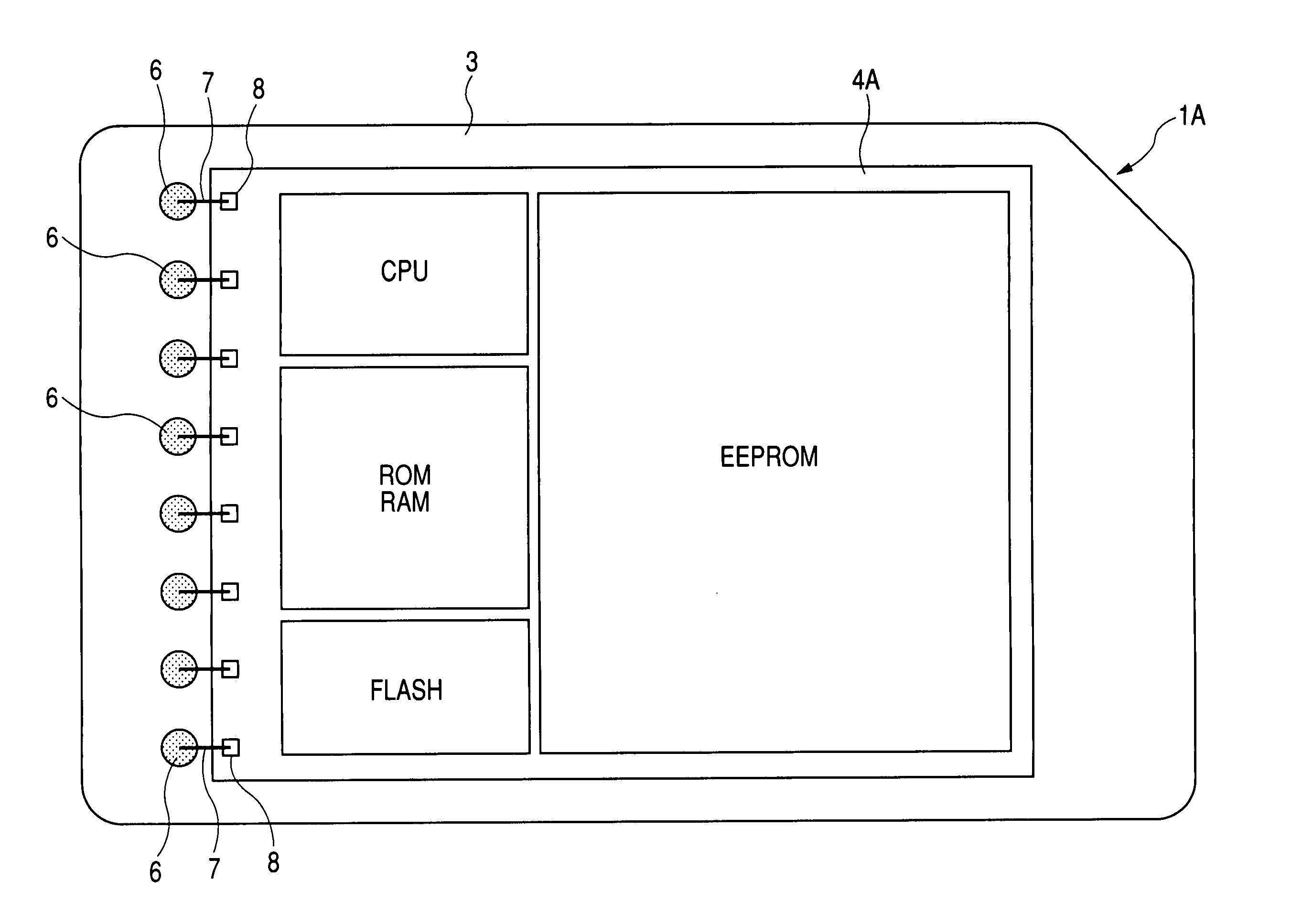
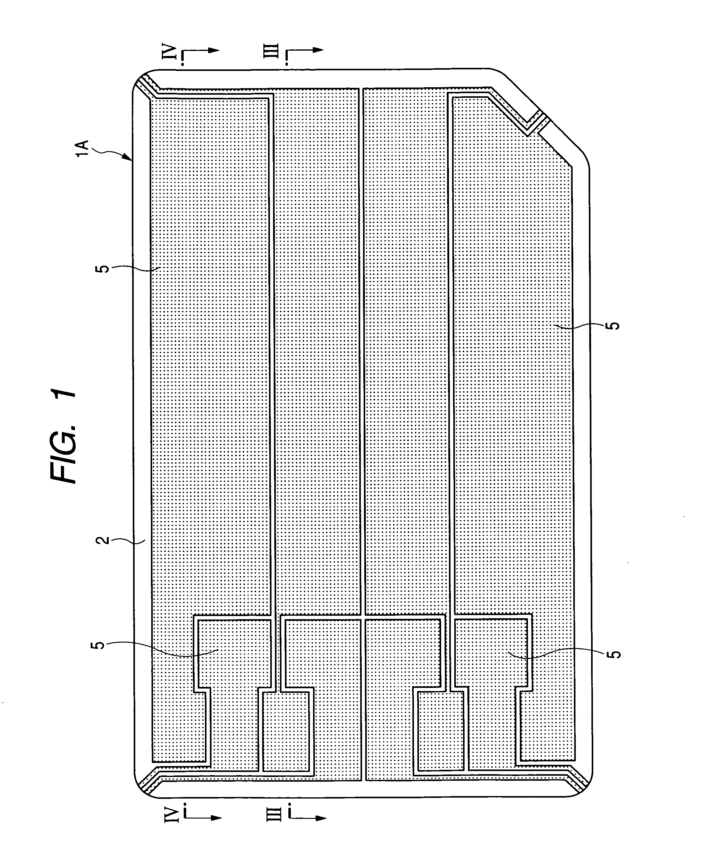
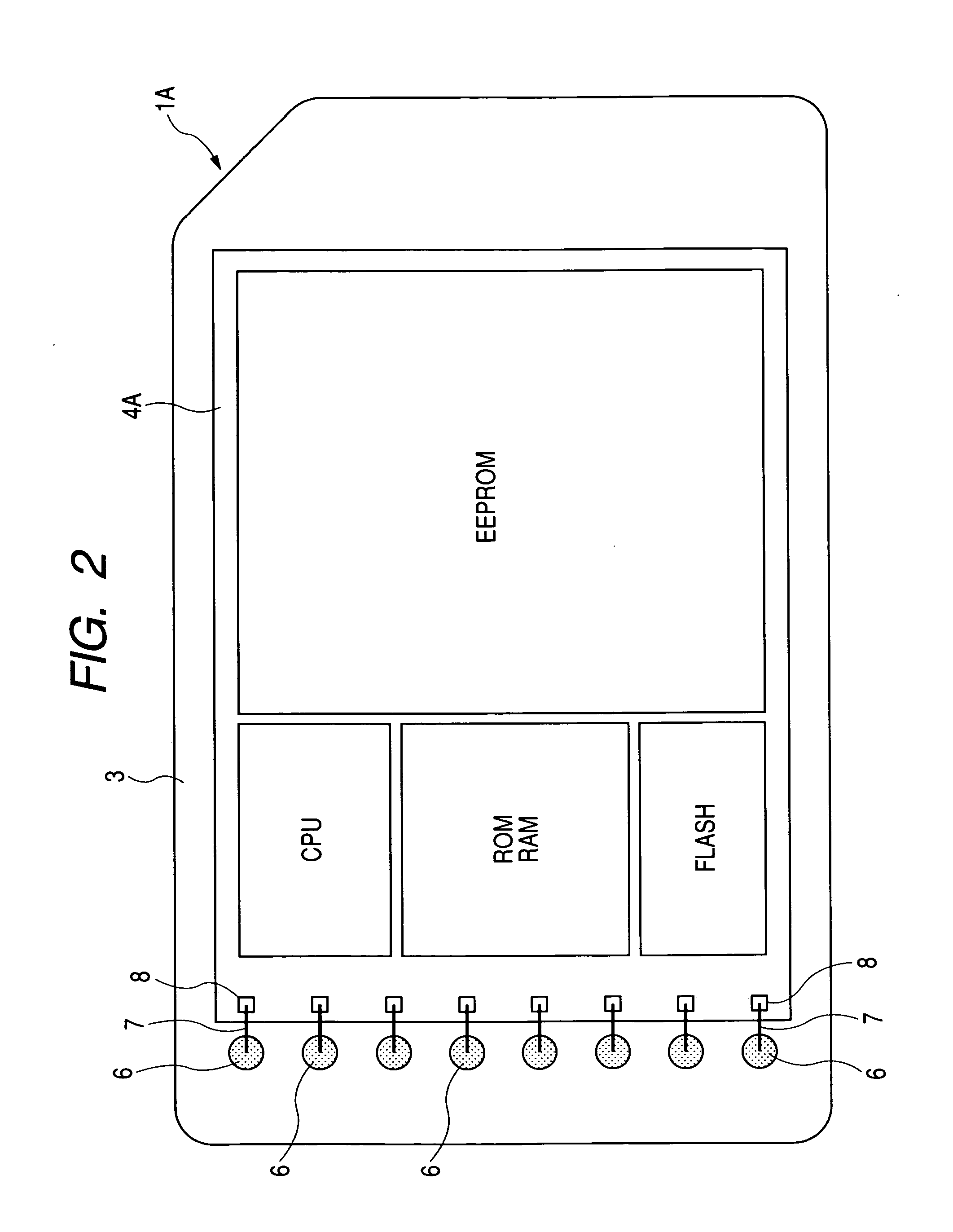
[0058]FIG. 1 is a plan view showing an example of the appearance of a plug-in UICC according to an embodiment of the present invention, FIG. 2 is a plan view showing an example of the internal structure of the plug-in UICC as seen from a back surface side thereof; FIG. 3 is a sectional view of the plug-in UICC taken on line III-III in FIG. 1; and FIG. 4 is a sectional view of the plug-in UICC taken along line IV-IV in FIG. 1.

[0059] The body of the plug-in UICC (1A) of this embodiment is constructed of a molding resin 2. A tape substrate 3 and a chip 4A mounted on one side of the tape substrate are sealed in the interior of the molding resin 2. The opposite side (opposite to the chip mounting side) of the tape substrate 3 is exposed to the exterior of the molding resin 2, and this opposite side constitutes a surface portion of the plug-in UICC (1A). Contact patterns 5, serving as external terminals of the plug-in UICC (1A), are formed on the surface of the t...

second embodiment

[0078] (Second Embodiment)

[0079]FIG. 17 is a plan view showing an example of the appearance of a plug-in UICC according to this second embodiment; FIG. 18 is a plan view showing an example of the internal structure of the plug-in UICC, as seen from a back surface side; and FIG. 19 is a sectional view of the plug-in UICC.

[0080] The plug-in UICC (1B) of this embodiment has a construction wherein a chip 4B and an oscillator 15 for a USB (Universal Serial Bus) are sealed in the interior of a body constructed of a molding resin 2. On one side of a tape substrate 3, with the chip 4B and the oscillator 15 for USB mounted thereon, there are wiring lines 16 connected to the oscillator 15 and also electrodes 17. The wiring lines 16 and the electrodes 17 are formed by etching Cu foil affixed to one side of an insulating film to form patterns and, thereafter, plating the surfaces of the patterns with Ni and Au.

[0081] The opposite side of the tape substrate 3 is exposed to the exterior of the ...


PUM


Abstract

A multi-function structure of a plug-in universal IC card is to be promoted and the manufacturing cost is to be reduced. The body of the plug-in UICC is constructed of a molding resin. A tape substrate and a chip mounted on one side of the tape substrate are sealed in the interior of the molding resin. A side opposite to the chip mounting side of the tape substrate is exposed to the exterior of the molding resin and constitutes a surface portion of the plug-in UICC. Contact patterns serving as external terminals of the plug-in UICC are formed on the surface of the tape substrate exposed to the exterior of the molding resin. In the plug-in UICC whose body is constructed of molding resin, cracking of the chip can be prevented effectively even in the case where the chip is large-sized.

Description

CROSS-REFERENCE TO RELATED APPLICATION [0001] The present application claims priority from Japanese Patent application JP 2003-318099, filed on Sep. 10, 2003, the content of which is hereby incorporated by reference into this application. BACKGROUND OF THE INVENTION [0002] The present invention relates to a method of manufacture of an integrated circuit (IC) card. Particularly, the present invention is concerned with a technique that is effective in the manufacture of a plug-in universal IC card for a portable telephone. [0003] Recently, a portable telephone, which utilizes a GSM (Global System for Mobile Communications) system, has enjoyed widespread use throughout the world. For using a portable telephone based on the GSM system, an SIM (Subscriber Identity Module) card, representing a kind of IC card that is issued by a portable telephone company and on which subscriber information is recorded, is inserted into the portable telephone. This portable telephone is advantageous in th...

Claims


Application Information

Patent Timeline
IPC IPC(8): B42D15/10G06K19/077
CPCG06K19/077H01L2224/48228G06K19/07724G06K19/07733G06K19/07743G06K19/07745H01L2224/48091H01L2924/01078H01L2924/01079H01L2924/19041G06K19/07718H01L2924/10253H01L2224/45144H01L2924/00014H01L2924/00H01L2224/49433
Inventor YAMADA, NOBUAKISUZUKI, KAZUNARIKURATOMI, BUNSHITANAKA, HIROAKIONOZAWA, AKIRA
Owner RENESAS ELECTRONICS CORP
Why Eureka
Try Eureka