Waveguide photodetector

a photodetector and waveguide technology, applied in the field of waveguide photodetectors, can solve the problems of difficult manufacturing such a structure, increase of capacitance, and ineffectiveness of semiconductor waveguides, and achieve the effects of low operating speed, high efficiency, and high operating speed

Inactive Publication Date: 2005-03-10
ELECTRONICS & TELECOMM RES INST
View PDF2 Cites 4 Cited by
  • Summary
  • Abstract
  • Description
  • Claims
  • Application Information

AI Technical Summary

Benefits of technology

[0019] The conventional waveguide photodetector has the problem that it is difficult to manufacture the waveguide photodetector due to the corresponding excessive etching. In addition, it has the problems that the operating speed is lowered under a high input power and it is difficult to select a central axis during a process for integrating the photodetector with the PLC. The present invention provides a waveguide photodetector solving these problems and having a high operating speed and a high efficiency.

Problems solved by technology

However, reduction of the thickness of the absorbing layer leads to the increase of the capacitance.
There are difficulties in manufacturing a semiconductor waveguide capable of effectively propagating the light beam having such a large diameter.
However, it is difficult to manufacture such a structure because it is deeply etched.
In other word, when the high power of light is incident, the operating speed is disadvantageously lowered.
In case of the structure in FIG. 1, a large amount of etching is necessary.
Therefore, when the waveguide photodetector is integrated with the PLC, its central axis is difficult to be accurately located, so that the effective coupling with the PLC may be difficult.

Method used


Image

  • Waveguide photodetector
  • Waveguide photodetector
  • Waveguide photodetector

Examples


Embodiment Construction

[0025] Now, the preferred embodiments of the present invention will be described in detail with reference to the accompanying drawings.

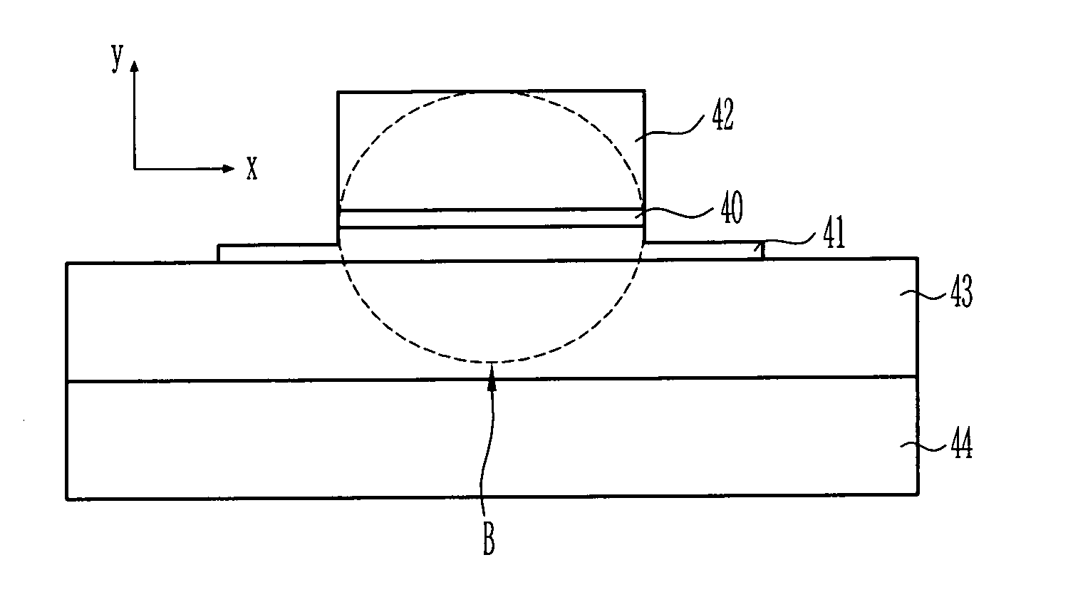
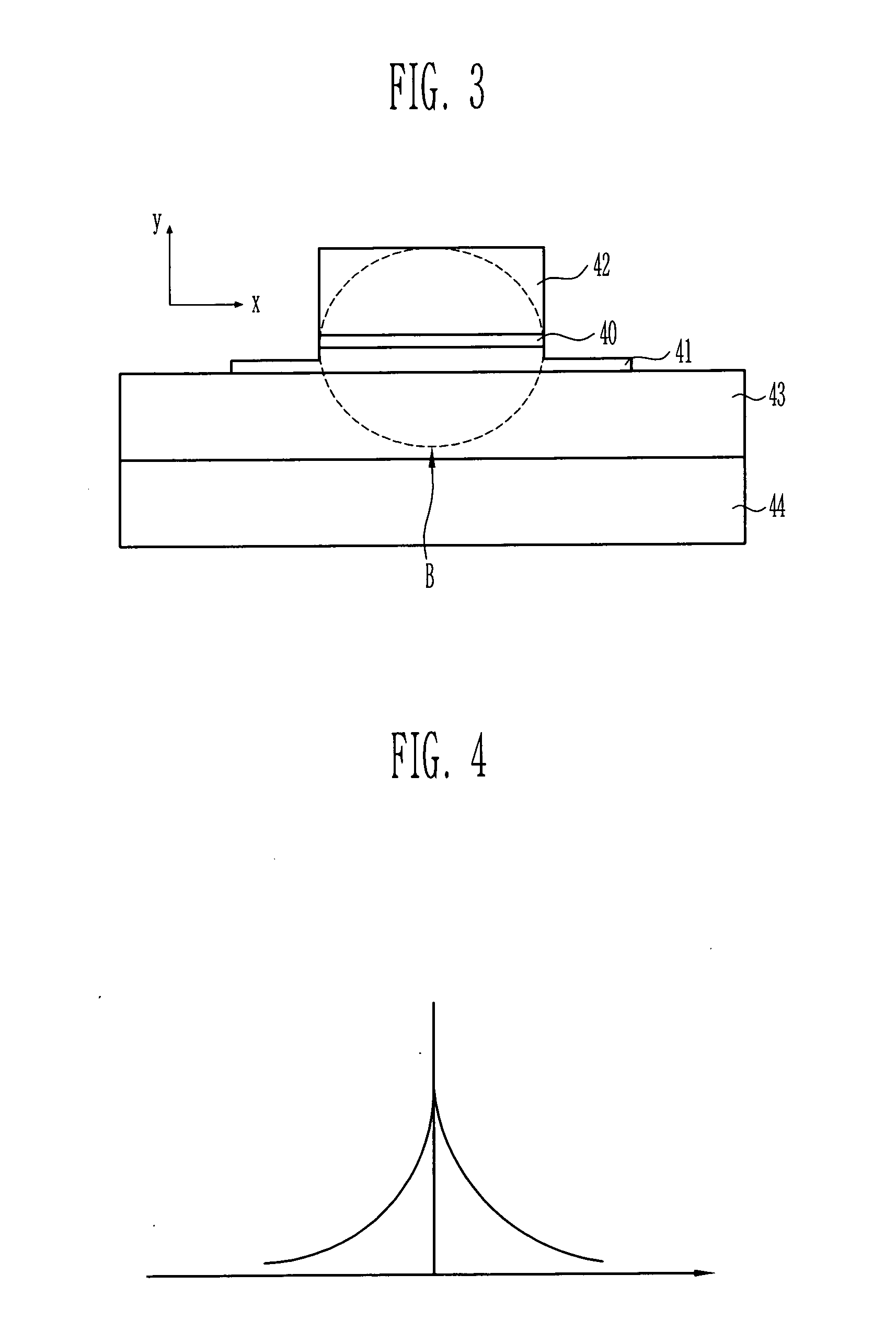
[0026]FIG. 3 is a cross-sectional view for explaining a waveguide photodetector according to the present invention.

[0027] An n-cladding layer 43, a non-doped spacer 41, an absorbing layer 40, and a p-cladding layer 42 are sequentially formed on a substrate 44. Predetermined portions of the p-cladding layer 42, the absorbing layer 40, and the spacer 41 are etched up to some depths, respectively. At that time, the depths of etching are adjusted, so that the central axis of light can be coincident with the central axis of the absorbing layer 40.

[0028] Band gap of the spacer 41 is larger than that of the absorbing layer 40 and smaller than or equal to that of the n-cladding layer43. Index of refraction of the spacer 41 is approximately equal to that of the absorbing layer 40 and larger than or equal to that of the n-cladding layer 43. The absorbing la...


PUM


Abstract

The present invention relates to a waveguide photodetector having a good efficiency of coupling with an optical fiber or a PLC (Planar Light-wave Circuit). In order to increase size of mode beam and to effectively receive light from the optical fiber or the PLC, a thin absorbing layer is used as a core and a semiconductor having an index of refraction similar to that of the absorbing layer is used as a cladding layer. By doing so, it is possible to obtain a good efficiency of coupling with an optical fiber or a PLC. In addition, since a little amount of light proceeds along a waveguide, it is possible to obtain high operating speed even under a high power. Furthermore, by reducing difference between indexes of refraction of the absorbing layer and the cladding layer, it is possible to suppress the “carrier-trapping” generated from small difference between band gaps of the two materials.

Description

BACKGROUND [0001] 1. Field of the Invention [0002] The present invention relates to a waveguide photodetector, and more specifically, a waveguide photodetector having a good efficiency of coupling with an optical fiber or a PLC (Planar Light-wave Circuit) and being capable of operating at a high speed under a high input power. [0003] 2. Discussion of Related Art [0004] The photodetector that converts an optical signal into an electrical signal is mainly manufactured with a semiconductor for which various kinds of semiconductor materials are used depending on usage of the photodetector. The photodetector manufactured with the semiconductor has a semiconductor absorbing layer which generates electrons and holes. The electrons and holes are moved into the respective electrodes to generate the electrical signal. [0005] As an example, there is a PIN diode photodetector. When a reverse voltage is applied to the photodetector, electrons and holes, that is, charges are generated and moved i...

Claims


Application Information

Patent Timeline
Patent Type & Authority Applications(United States)
IPC IPC(8): G02B6/12G02B6/122G02B6/42
CPCG02B6/4202G02B6/122G02B6/12
Inventor PARK, JUNG WOOBAEK, YONG SOON
Owner ELECTRONICS & TELECOMM RES INST
Why Eureka
Try Eureka