Method for simultaneous degas and baking in copper damascene process

a technology of damascene and copper, which is applied in the direction of semiconductor/solid-state device manufacturing, basic electric elements, electric devices, etc., can solve the problems of copper not being able to successfully etch to form metal lines, affecting the wafer throughput of separate furnace baking methods, and presenting significant slowdowns in wafer throughpu

Active Publication Date: 2005-03-10
TAIWAN SEMICON MFG CO LTD
View PDF4 Cites 39 Cited by
  • Summary
  • Abstract
  • Description
  • Claims
  • Application Information

AI Technical Summary

Problems solved by technology

The use of copper, however, has presented several technical manufacturing problems that must be overcome for successful implementation of the technology.
For example, copper cannot be successfully etched to form metal lines since it does not form volatile components with known etching chemistry's.
One difficulty with prior art copper damascene processes is the process involving etching through an etch stop layer at a via bottom portion to form closed communication with an underlying copper region and the subsequent process of barrier layer depositio...

Method used


Image

  • Method for simultaneous degas and baking in copper damascene process
  • Method for simultaneous degas and baking in copper damascene process
  • Method for simultaneous degas and baking in copper damascene process

Examples


Embodiment Construction

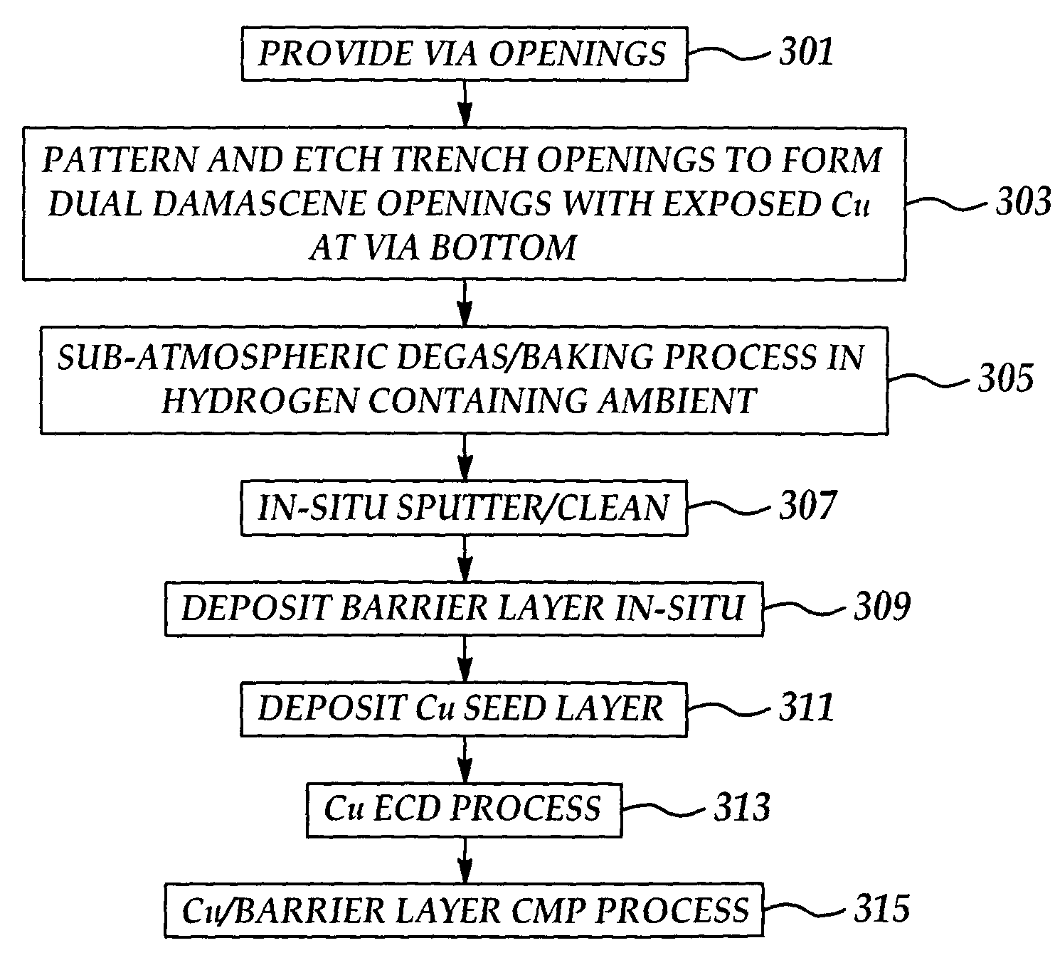
[0014] Although the method of the present invention is explained with reference to and is particularly advantageously implemented on forming of copper dual damascenes it will be appreciated that the method of the present invention is equally applicable to the formation of single copper damascenes and relatively thick and wide copper damascene structures including, for example, bonding pads or wide trench lines.

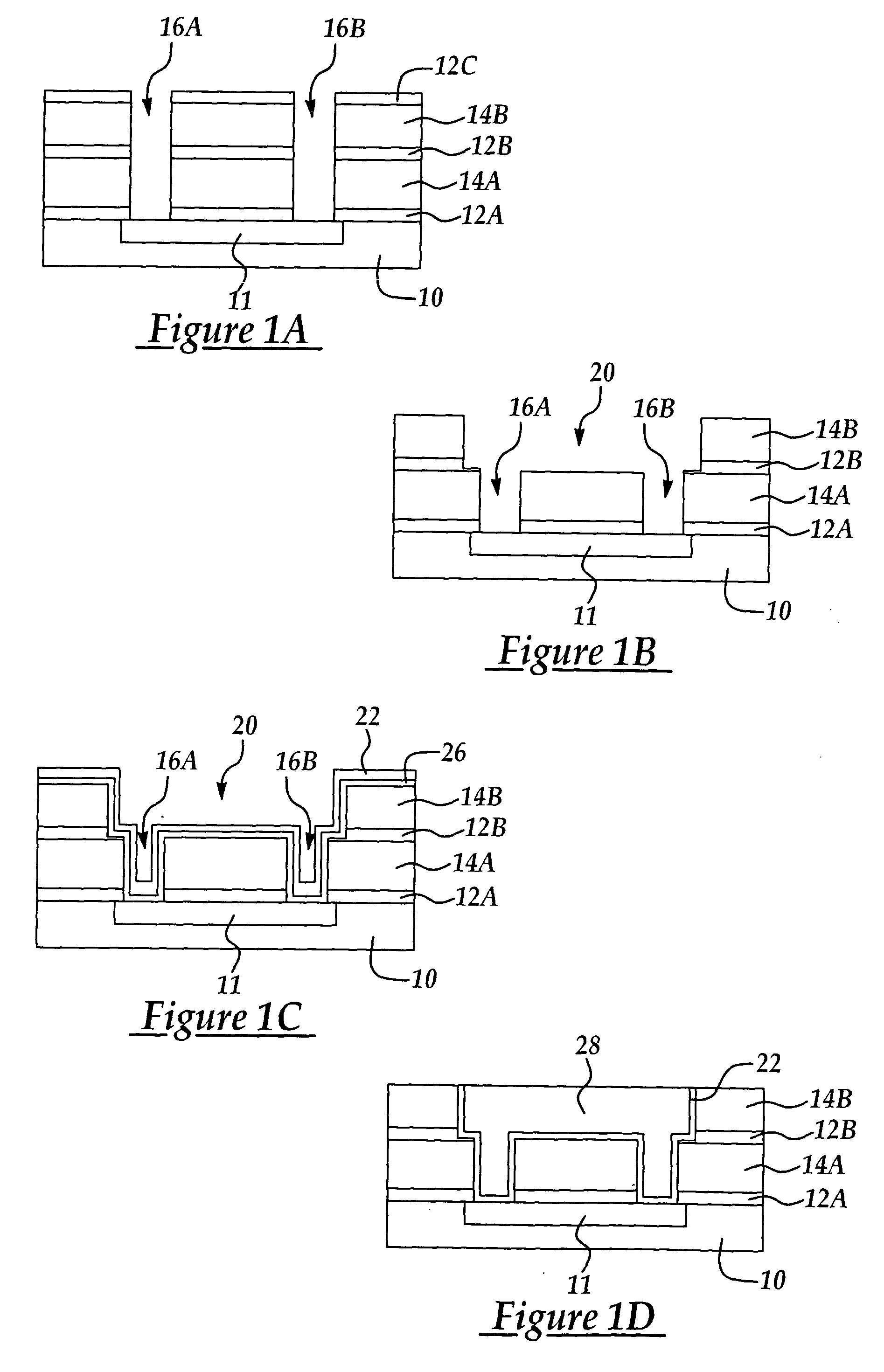
[0015] In an exemplary embodiment of the present invention, reference is made to FIGS. 1A-1D where cross sectional side views of a portion of a multi-level semiconductor device is shown at stages of manufacture according to an exemplary dual damascene process according to an embodiment the invention.

[0016] Shown in FIG. 1A is a lowermost first etch stop layer 12A, formed over a copper region 11, formed in dielectric insulating layer 10. The first etch stop layer 12A, preferably formed of silicon nitride or silicon carbide, for example, by an LPCVD or PECVD process, is formed...


PUM


Abstract

A method for forming a copper damascene feature including providing a semiconductor process wafer including at least one via opening formed to extend through a thickness of at least one dielectric insulating layer and an overlying trench line opening encompassing the at least one via opening to form a dual damascene opening; etching through an etch stop layer at the at least one via opening bottom portion to expose an underlying copper area; carrying out a sub-atmospheric DEGAS process with simultaneous heating of the process wafer in a hydrogen containing ambient; carrying out an in-situ sputter-clean process; and, forming a barrier layer in-situ to line the dual damascene opening.

Description

FIELD OF THE INVENTION [0001] This invention generally relates to semiconductor processing methods for forming metal contacts in a multilevel semiconductor device and more particularly a method for forming copper damascene features with reduced number of processing steps. BACKGROUND OF THE INVENTION [0002] Formation of multi-level semiconductor devices entails the formation of multiple levels of metal interconnects such as vias and trench lines (local interconnect lines). For example, in a multi-level semiconductor device there are frequently formed several layers of vias interconnecting wider metal interconnect line portions among the multiple layers or levels of the device. Frequently, several vias will connect a wider metal portion, for example a bonding pad in an uppermost metallization layer to an underlying metallization level through several relatively narrower vias. For example the vias and metal interconnect lines are typically formed with line widths having a dimensions of...

Claims


Application Information

Patent Timeline
IPC IPC(8): H01L21/285H01L21/3105H01L21/311H01L21/768
CPCH01L21/28556H01L21/3105H01L21/76807H01L21/76873H01L21/76838H01L21/76843H01L21/76814
Inventor PAN, SHING-CHYANGHSIEH, CHING-HUALIN, JING-CHENGLEE, HSIEN-MINGHUANG, CHENG-LINSHUE, SHAU-LIN
Owner TAIWAN SEMICON MFG CO LTD
Why Eureka
Try Eureka