Circuit device and manufacturing method of circuit device

a manufacturing method and circuit device technology, applied in the field of circuit devices, can solve the problems of too large total size to meet the requirements of smaller, thinner and lighter requirements, difficult to provide an electrical circuit device in size, thickness and weight reduction, etc., and achieve the effect of preventing slipping

Inactive Publication Date: 2005-03-17
SANYO ELECTRIC CO LTD
View PDF27 Cites 24 Cited by
  • Summary
  • Abstract
  • Description
  • Claims
  • Application Information

AI Technical Summary

Benefits of technology

[0071] forming a circuit by removing uniformly said conductive foil at a portion of thickness where said trench is not provided from the back side and making the back face of said conductive paths and said insulating resin across said trench a substantially flat surface, to enable a...

Problems solved by technology

However, this package type semiconductor device 1 had the lead terminal 4 out of the resin layer 3, and was too large in total size to meet smaller, thinner and lighter requirements.
Thereafter, the same manufacturing method of FIG. 26, up to coating the resin layer is followed, but since the ceramic substrate is very fragile, and is likely to break off, unlike a flexible sheet or the glass epoxy substrate, there is a problem with the difficulty of molding using die.
However, only these components were difficult to provide an electrical circuit device reduced in size, thickness and weight.
However, since the manufacturing method involves pasting the electrode on the subs...

Method used


Image

  • Circuit device and manufacturing method of circuit device
  • Circuit device and manufacturing method of circuit device
  • Circuit device and manufacturing method of circuit device

Examples


first embodiment

[0130] First Embodiment for Circuit Device

[0131] Referring to FIG. 1, a circuit device of the present invention will be first described below in connection with its structure.

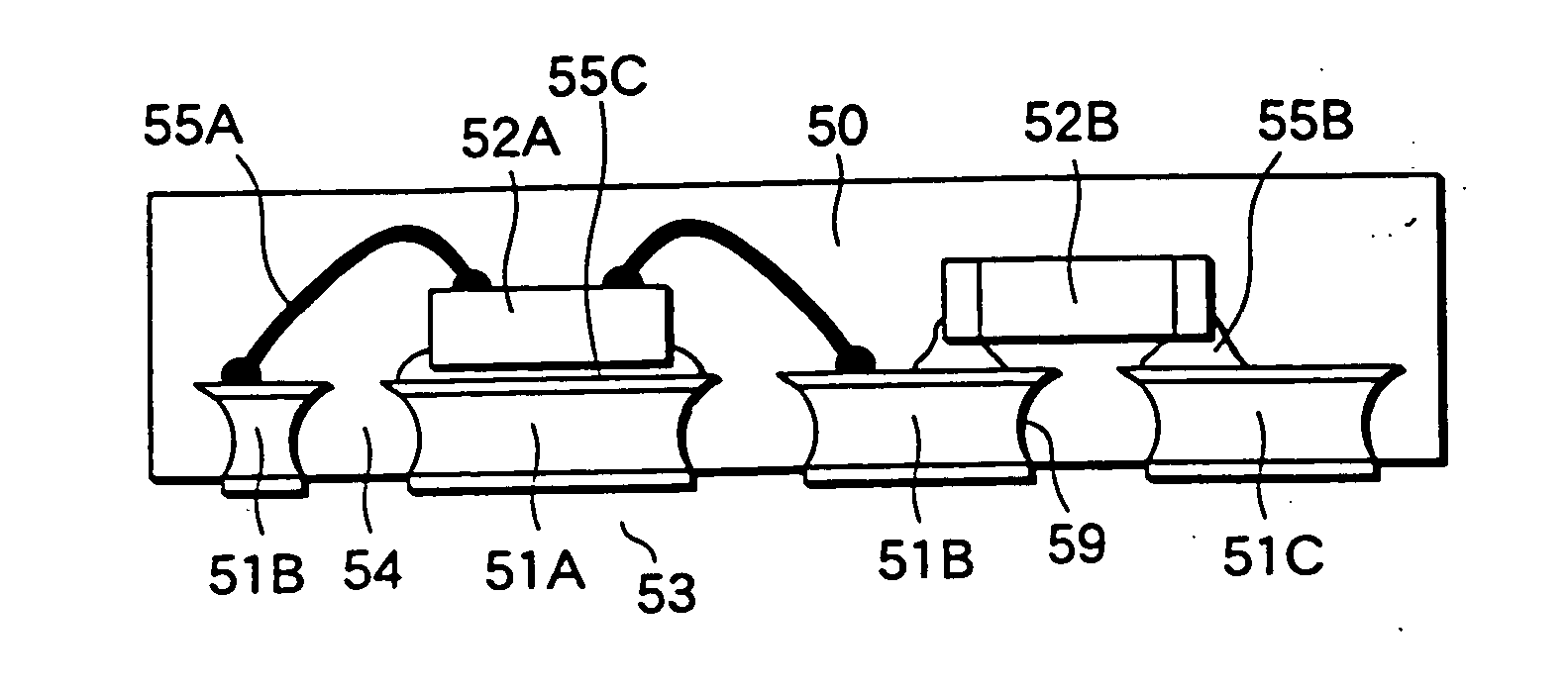
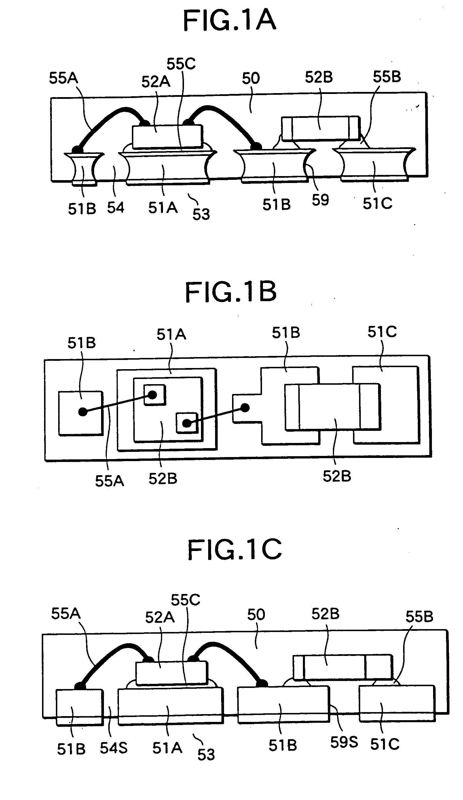
[0132]FIG. 1 shows a circuit device 53 in which a conductive path 51 is buried into an insulating resin 50, and a circuit device 52 is fixed on said conductive path 51 supported by the insulating resin 50. The lateral face of the conductive path 51 has a curved structure 59.

[0133] This circuit device is mainly composed of the circuit elements 52A, 52B, a plurality of conductive paths 51A, 51B and 51C, and the insulating resin 50 into which the conductive paths 51A, 51B and 51C are buried. Between the conductive paths 51, a trench 54 is filled with the insulating resin 50. And the insulating resin 50 supports the conductive paths 51 of the curved structure 59.

[0134] The insulating resin may be a thermosetting resin, such as epoxy resin, or a thermoplastic resin, such as polyimide resin and polyphenylene sulfi...

second embodiment

[0150] Second Embodiment for Circuit Device

[0151] A circuit device 53 of FIG. 2 will be described below.

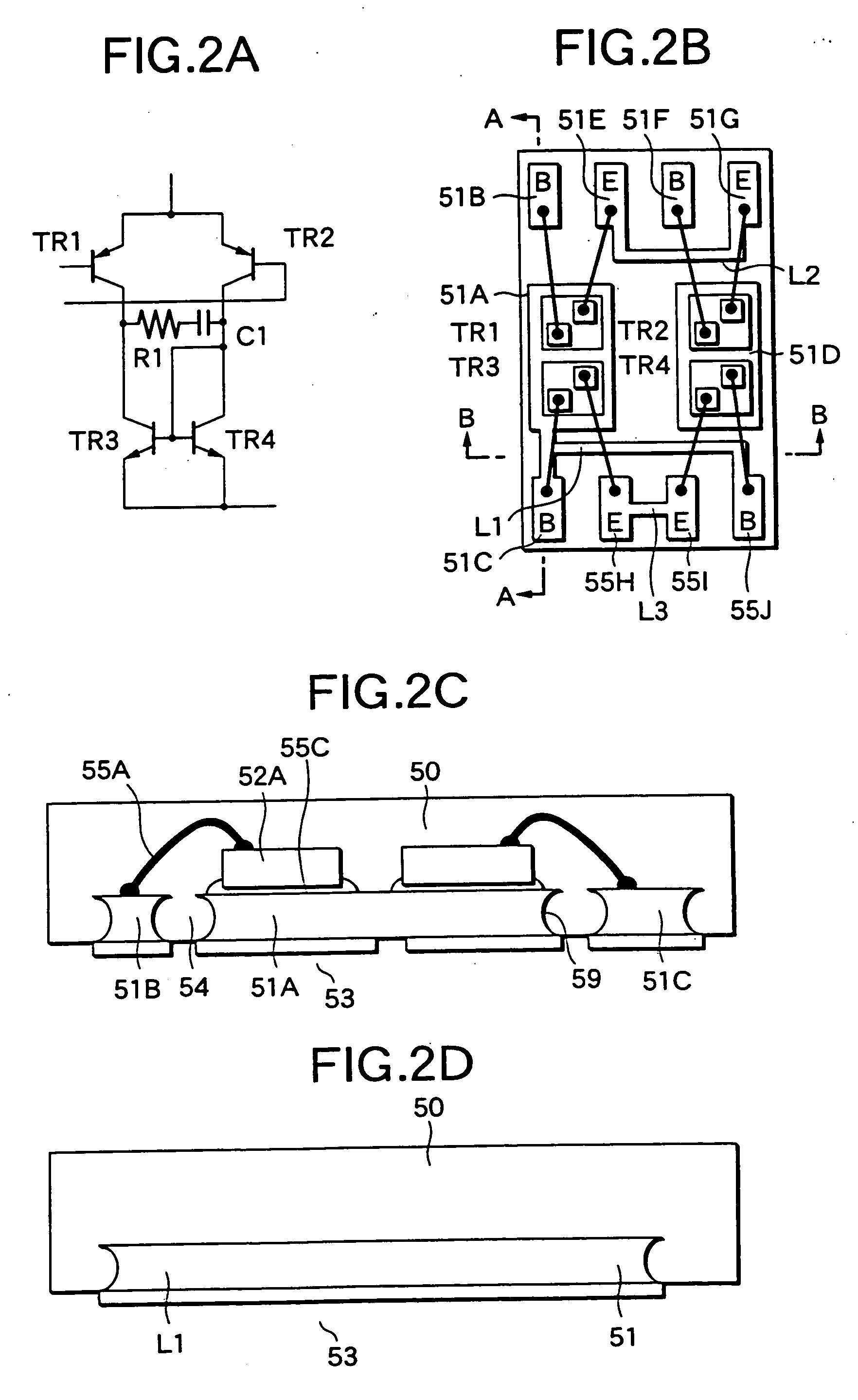
[0152] This circuit device has substantially the same structure as that of FIG. 1, except that the interconnects L1 and L2 are formed as the conductive paths 51. Accordingly, the interconnects L1 and L2 will be described below.

[0153] As described before, there are a wide variety of IC circuits from a small-scale circuit to a large-scale circuit. For the convenience of the drawings, the small-scale circuit is only shown in FIG. 2A. This circuit is most applicable to an audio amplifying circuit having a difference amplifying circuit and a current mirror circuit connected. The difference amplifying circuit is constituted of a TR1 and a TR2, and the current mirror circuit is constituted of a TR3 and a TR4, as shown in FIG. 2A.

[0154]FIG. 2B is a plan view of the circuit device to which the circuit of FIG. 2A is applied. FIG. 2C is a cross-sectional view taken along the line A-A in F...

third embodiment

[0158] Third Embodiment for Circuit Device

[0159] A circuit device 56 of FIG. 8 will be described below.

[0160] This circuit device has substantially the same structure of FIG. 1 or 2, except that a conductive coat 57 is formed on the surface of the conductive paths 51. Herein, the conductive coat 57 on the conductive paths will be mainly described below.

[0161] A first feature is to provide the conductive coat 57 to prevent the circuit device or the conductive path 51 from warping.

[0162] Typically, due to a difference in thermal expansion coefficient between the insulating resin and the conductive path material (hereinafter referred to as a first material) the circuit device itself may be warped, or the conductive path curved or peeled. Since the thermal conductivity of the conductive paths 51 is superior to that of the insulating resin, the conductive paths 51 will rise in temperature more rapidly, and expand. A second material having a smaller thermal expansion coefficient than t...


PUM


Abstract

After a trench 54 is formed in a conductive foil 60, the circuit elements are mounted, and the insulating resin is applied on the conductive foil 60 as the support substrate. After being inverted, the conductive foil 60 is polished on the insulating resin 50 as the support substrate for separation into the conductive paths. Accordingly, it is possible to fabricate the circuit device in which the conductive paths 51 and the circuit elements 52 are supported by the insulating resin 50, without the use of the support substrate. And the interconnects L1 to L3 requisite for the circuit are formed, and can be prevented from slipping because of the curved structure 59 and a visor 58.

Description

BACKGROUND OF THE INVENTION [0001] 1. Field of the Invention [0002] The present invention relates to a circuit device and a method for manufacturing the circuit device, and more particularly to a thin-type circuit device and a method of manufacturing the thin-type circuit device without the need of providing a support substrate. [0003] 2. Description of the Related Art [0004] Conventionally, it has been demanded that a circuit device which is set in an electronic apparatus is reduced in size, thickness and weight, because the circuit device is used for a portable telephone, a portable computer and so on. [0005] For example, a semiconductor device as a circuit device is typically a package type semiconductor device which is conventionally sealed by normal transfer molding. This semiconductor device 1 is mounted on a printed circuit board PS as shown in FIG. 24. [0006] This package type semiconductor device 1 has a semiconductor chip 2 covered with a resin layer 3, with a lead termina...

Claims


Application Information

Patent Timeline
IPC IPC(8): H05K1/02H01L21/48H01L21/56H01L21/98H01L23/31H01L25/10H01L25/16H05K1/18H05K3/06H05K3/20
CPCH01L21/4821H01L2924/07802H01L21/56H01L23/3107H01L24/45H01L24/48H01L24/97H01L25/105H01L25/165H01L25/50H01L2221/68377H01L2224/16H01L2224/32245H01L2224/45144H01L2224/48091H01L2224/48227H01L2224/48245H01L2224/48247H01L2224/48464H01L2224/48465H01L2224/48599H01L2224/49171H01L2224/73265H01L2224/85439H01L2224/97H01L2924/01005H01L2924/01006H01L2924/01013H01L2924/01014H01L2924/01028H01L2924/01029H01L2924/01033H01L2924/01046H01L2924/01047H01L2924/0105H01L2924/01059H01L2924/01078H01L2924/01079H01L2924/01082H01L2924/01083H01L2924/014H01L2924/09701H01L2924/13055H01L2924/14H01L2924/19041H01L2924/19043H01L2924/19105H05K1/187H05K1/188H05K3/06H05K3/202H01L24/49H01L2224/32225H01L2924/01024H01L2924/19106H01L25/0655H01L2924/3511H01L2224/45124H01L2225/1029H01L2924/15311H01L2924/10253H01L21/4832H01L2924/00014H01L2224/85H01L2224/83H01L2924/00H01L2924/00012H01L24/29H01L24/32H01L24/73H01L24/83H01L2224/05554H01L2224/29101H01L2224/2929H01L2224/29339H01L2224/45139H01L2224/48639H01L2224/48739H01L2224/83815H01L2224/83851H01L2224/85205H01L2924/00011H01L2924/10161H01L2924/12042H01L2924/15747H01L2924/15787H01L2924/181H01L2924/07811H01L2224/83205H01L2224/45015H01L2924/207H05K1/18
Inventor SAKAMOTO, NORIAKIKOBAYASHI, YOSHIYUKISAKAMOTO, JUNJIMASHIMO, SHIGEAKIOKAWA, KATSUMIMAEHARA, EIJUTAKAHASHI, KOUJI
Owner SANYO ELECTRIC CO LTD
Why Eureka
Try Eureka