Temperature compensated, high efficiency, controlled input impedance diode detector

a diode detector and input impedance technology, applied in the field of diode detector circuits, can solve the problems of complex circuit design, poor thermal stability of the circuit, and high cost, size, weight, and power requirements of the differential amplifier,

Inactive Publication Date: 2005-03-17
VECTRON INT INC
View PDF10 Cites 19 Cited by
  • Summary
  • Abstract
  • Description
  • Claims
  • Application Information

AI Technical Summary

Benefits of technology

The invention is usable in many applications including when embedded within any integrated circuit, for bolometers, as demodulators in radio devices, and most specifically in digital radio or in Automatic Gain Control (AGC) or Automatic Level Control (ALC) circuits that are specially sensitive when used for Quadrature Amplitude Modulation (QAM). Uses also extend to spectrum analyzer and similar instrumentation. A significant advantage of the invention is the ability to place a passive, sensitive, temperature compensated detector in a harsh environment at the terminal end of a cable while obtaining sufficient signal integrity at the active electronic processing circuitry, located remotely from the harsh environment. This capability addresses not only passive detection of RF signals, but also power level and insertion loss measurements in sensors based on the propagation of RF, sonic, subsonic or ultrasonic signals in piezoelectric devices and other ultrasonic sensor devices.
is the ability to place a passive, sensitive, temperature compensated detector in a harsh environment at the terminal end of a cable while obtaining sufficient signal integrity at the active electronic processing circuitry, located remotely from the harsh environment. This capability addresses not only passive detection of RF signals, but also power level and insertion loss measurements in sensors based on the propagation of RF, sonic, subsonic or ultrasonic signals in piezoelectric devices and other ultrasonic sensor devices.

Problems solved by technology

The circuit however, suffers from poor thermal stability.
While the circuit of FIG. 2 offers temperature compensation, the cost, size, weight, and power requirements of the differential amplifier are prohibitive for many applications.
The need for positive 24 and negative 22 power supplies further complicates circuit design, and is in stark contrast to the passive nature of the circuit of FIG. 1.
Furthermore, the differential amplifiers typically have restricted operating temperature range, whereas the passive components operate over much larger temperature extremes.
However, the Tamura circuit suffers a major drawback: Due to the voltage divider, the circuit provides only one half of the voltage provided by a single diode, non-compensated detector.
As the Eriksson system is also based on a voltage divider, it suffers from a 50% (6 dB) decrease in detection efficiency over the single diode detector, which like the Tamura circuit translates into lower dynamic range and lower signal to noise ratio.
When measured with a differential amplifier the Waugh circuit provides good temperature stability but again suffers from the disadvantages of low efficiency and the use of a differential amplifier entails all the liabilities mentioned above.
However, at relatively high signal input levels the input resistance at RF becomes a significant and variable load to the RF circuit.

Method used


Image

  • Temperature compensated, high efficiency, controlled input impedance diode detector
  • Temperature compensated, high efficiency, controlled input impedance diode detector
  • Temperature compensated, high efficiency, controlled input impedance diode detector

Examples


Embodiment Construction

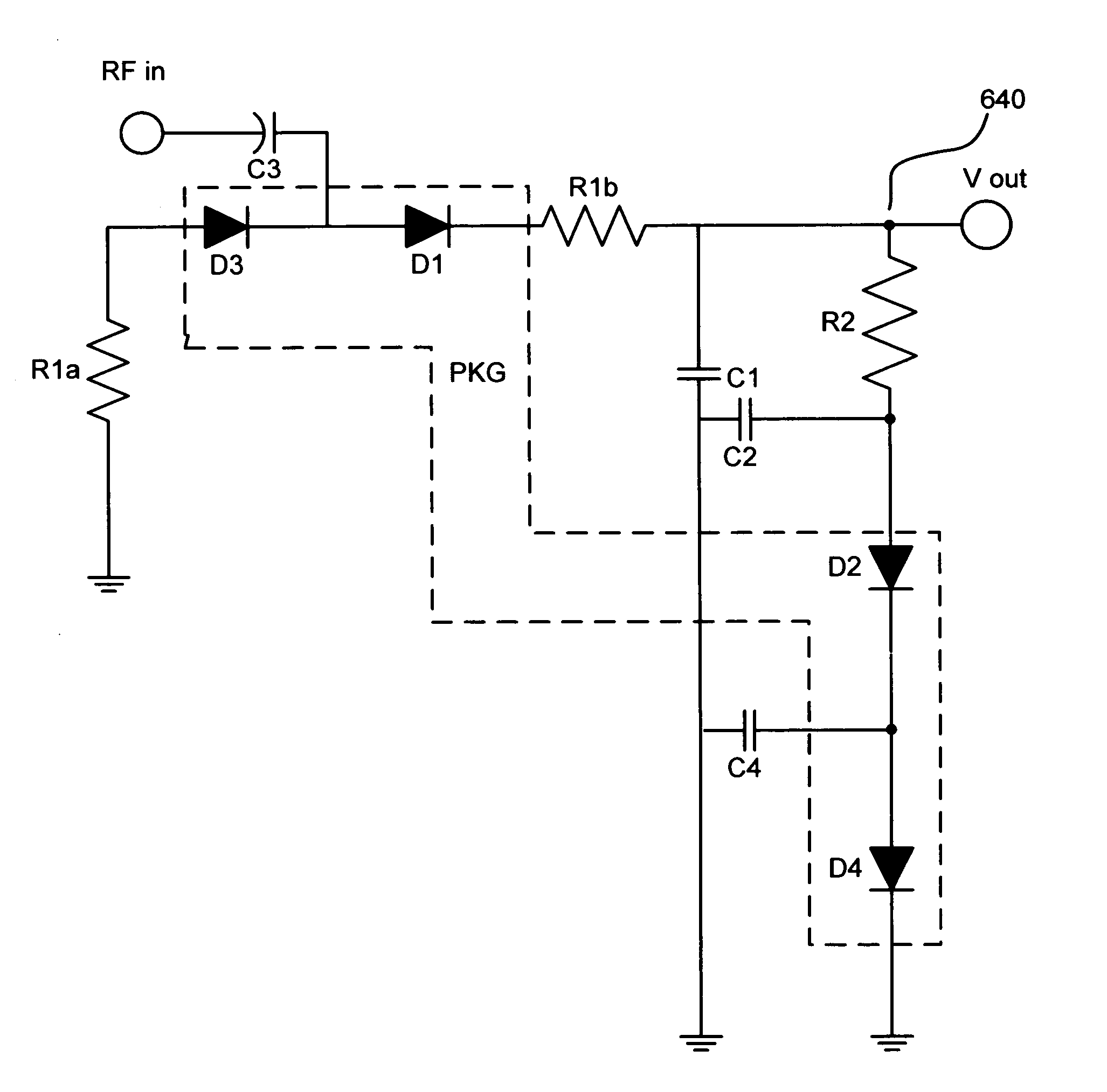
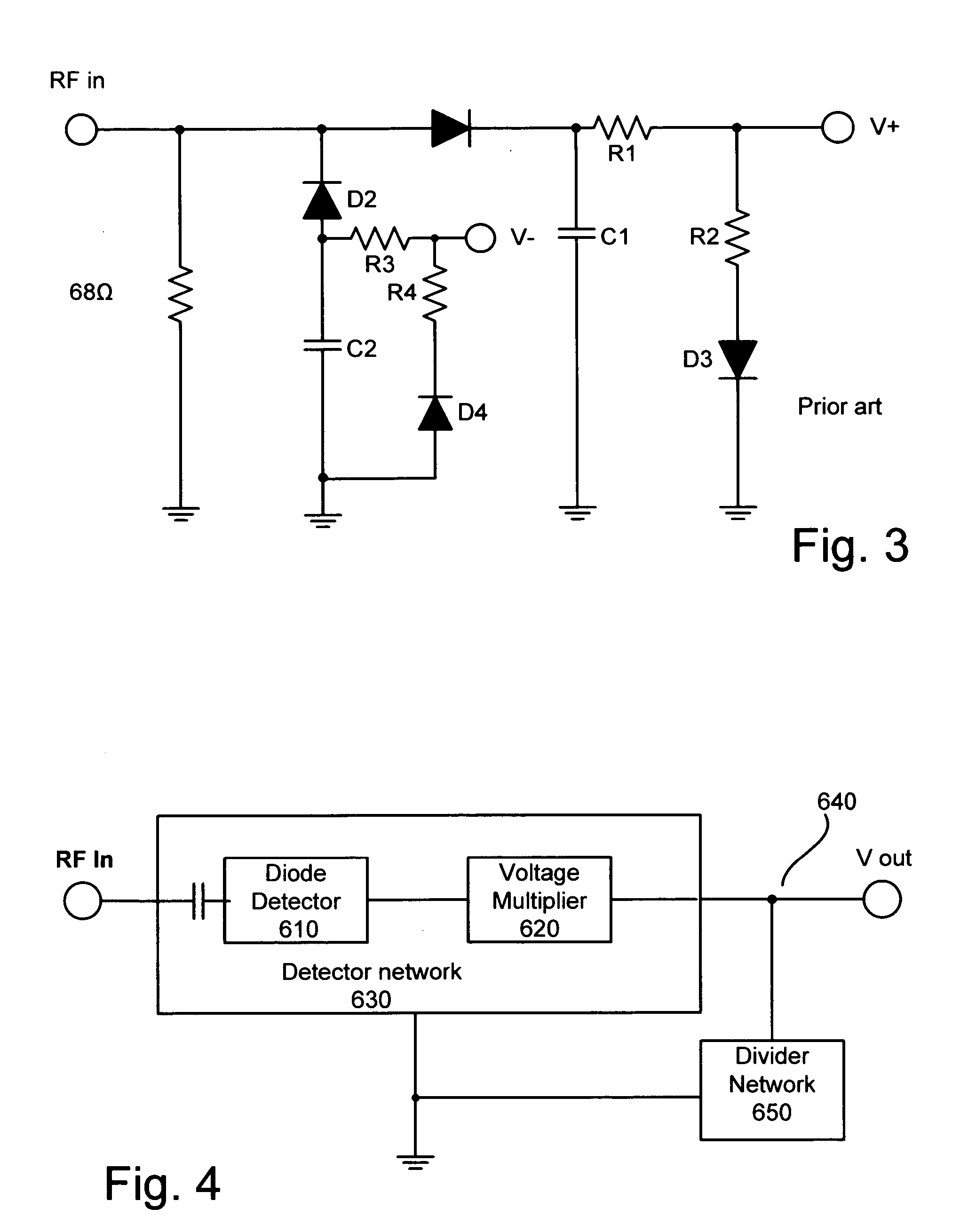
Referring now to FIG. 4 a most basic embodiment of the invention disclosed in Ser. No. 10 / 429,151 is shown. An RF (or any frequency) signal is inputted via input terminal RFin, into detector network 630. Detector network 630 comprises at least two basic components—a diode detector 610 and a voltage multiplier 620. Those skilled in the art will recognize that the diode used in the diode detector 610 may be utilized as a part of the voltage multiplier 620, or the detector may be separate from the voltage multiplier. In the preferred embodiment the voltage multiplier is a voltage doubler, comprising of the detector diode and a multiplier diode, however any number of diodes may be used, to provide voltage multiplication of any factor.

Divider network 650 is coupled to the output of the detector network at junction 640, and as it is coupled to the circuit ground (equivalently referred to as ground in these specifications), it forms a voltage divider together with the detector network. ...


PUM


Abstract

A diode detector comprising a detector network adapted to detect and multiply the detected voltage coupled to a divider network that comprise diodes in equal number to the number of diodes in the detector network, provides a passive detector applicable to any application requiring a small, efficient, high output, inexpensive temperature compensated detector for use as demodulator or as power to voltage converter. Integrating a portion of the divider network in the detector / multiplier network allows control over the minimum input impedance of the detector.

Description

FIELD OF THE INVENTION This invention relates to diode detector circuits and more particularly to a passive, temperature compensated high efficiency diode detector BACKGROUND OF THE INVENTION Diode detectors had been known in the art from the first days of radio. They are used to demodulate radio frequency (RF) or any other alternating current (AC) signal and turn it into voltage representative of the modulating waveform. A common diode detector is shown in FIG. 1. AC, sonic, sub sonic, ultra sonic or RF energy and the like (commonly referred to as RF hereinafter) is rectified by diode D1 that acts as a non-linear element for the conversion. While a Schottky diode is preferred, alternative asymmetric junctions are also suitable. The rectified signal is integrated by the capacitor C1 which also serves as the ground return path for the RF signal. Additional components are frequently included to improve functionality. By way of example, inductor L1 may be employed to provide electri...

Claims


Application Information

Patent Timeline
Patent Type & Authority Applications(United States)
IPC IPC(8): H03D1/10
CPCH03D1/10
Inventor ANDLE, JEFFREY C.
Owner VECTRON INT INC
Why Eureka
Try Eureka