Systems and methods for processing thin films

a technology of thin film and processing method, applied in semiconductor/solid-state device testing/measurement, manufacturing tools, instruments, etc., can solve the problems of consuming a lot of energy, so as to reduce the cost of manufacturing thin films and reduce the price per shot/pulse , the effect of efficient utilization of energy

Inactive Publication Date: 2005-03-17
THE TRUSTEES OF COLUMBIA UNIV IN THE CITY OF NEW YORK
View PDF98 Cites 120 Cited by
  • Summary
  • Abstract
  • Description
  • Claims
  • Application Information

AI Technical Summary

Benefits of technology

[0011] Laser systems are capable of generating laser beam pulses that have sufficient energy and pulse durations to process more than one thin film sample at a time. To efficiently utilize the generated laser beam pulses to process thin film samples, such laser beam pulses can be split into component laser beam pulses. Thin film samples can then be irradiated with the component laser beam pulses. By generating and splitting laser beam pulses that have sufficient energy and pulse durations to process more than one thin film sample at a time, the energy generated by the laser system can be more efficiently utilized in processing the thin film samples. By efficiently utilizing the energy that is produced by the laser system, the manufacturing costs for producing thin films can be reduced, e.g., the price per shot / pulse can be reduced.

Problems solved by technology

ELA produces homogeneous small grained polycrystalline films; however, the method often suffers from microstructural non-uniformities which can be caused by pulse to pulse energy density fluctuations and / or non-uniform beam intensity profiles.
In addition, it may take approximately 200 second to 600 seconds to completely process the semiconductor film sample using the ELA techniques, without even taking into consideration the time it takes to load and unload such sample.
Such stability may be reduced or compromised when the pulsed beams are turned off or shut down, and then restarted.
In addition, the costs associated with processing semiconductor samples are generally correlated with the number of pulses emitted by the beam source.

Method used


Image

  • Systems and methods for processing thin films
  • Systems and methods for processing thin films
  • Systems and methods for processing thin films

Examples


Embodiment Construction

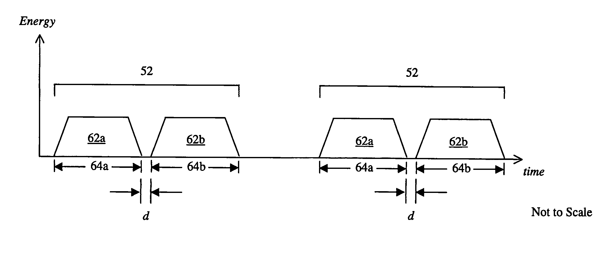
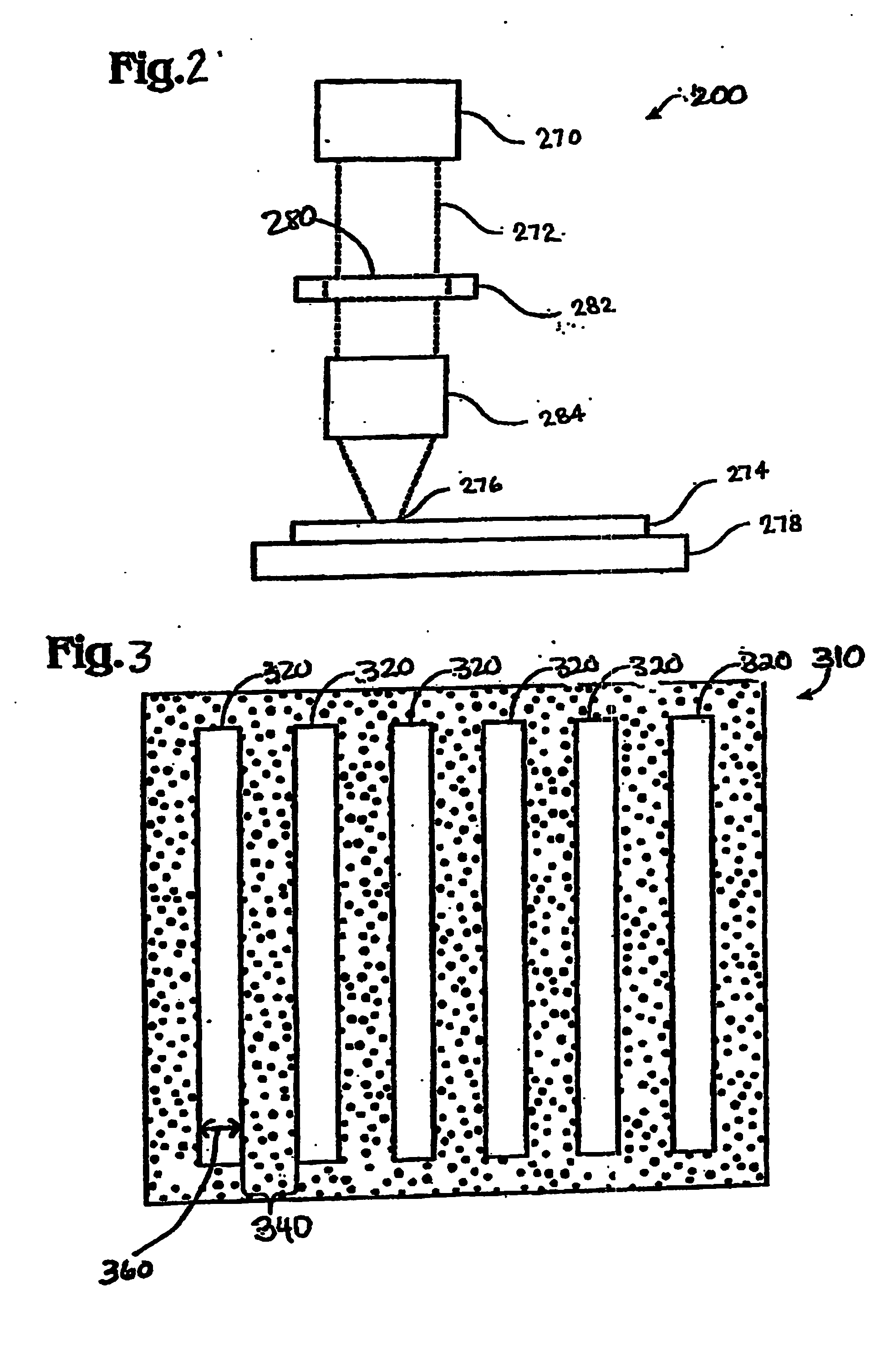
[0042] The quality of a film that has been crystallized using a laser-induced crystallization growth technique depends, in part, on the energy beam characteristics of the laser beam pulse that is used to irradiate the film and in the manner in which these laser beams are delivered, e.g., continuous scan, two-shot, n-shot, to the film. This observation is used to crystallize different regions of the films with laser beams having different energy beam characteristics in an energy- and time-efficient manner and to provide the film performance characteristics needed in device to be fabricated. Laser-induced crystallization is typically accomplished by laser irradiation using a wavelength of energy that can be absorbed by the film. The laser source may be any conventional laser source, including but not limited to, excimer laser, continuous wave laser and solid-state laser. The irradiation beam pulse can be generated by another known source or short energy pulses suitable for melting a s...


PUM

PropertyMeasurementUnit
transfer timeaaaaaaaaaa
lengthaaaaaaaaaa

Abstract

The present disclosure is directed to methods and systems for processing a thin film samples. In an exemplary method, semiconductor thin films are loaded onto two different loading fixtures, laser beam pulses generated by a laser source system are split into first laser beam pulses and second laser beam pulses, the thin film loaded on one loading fixture is irradiated with the first laser beam pulses to induce crystallization while the thin film loaded on the other loading fixture is irradiated with the second laser beam pulses. In a preferred embodiment, at least a portion of the thin film that is loaded on the first loading fixture is irradiated while at least a portion of the thin film that is loaded on the second loading fixture is also being irradiated. In an exemplary embodiment, the laser source system includes first and second laser sources and an integrator that combines the laser beam pulses generated by the first and second laser sources to form combined laser beam pulses. In certain exemplary embodiments, the methods and system further utilize additional loading fixtures for processing additional thin film samples. In such methods and systems, the irradiation of thin film samples loaded on some of the loading fixtures can be performed while thin film samples are being loaded onto the remaining loading fixtures. In certain exemplary methods and systems, the crystallization processing of the semiconductor thin film samples can consist of a sequential lateral solidification (SLS) process.

Description

CROSS-REFERENCE TO RELATED APPLICATIONS [0001] This patent application claims priority to U.S. Provisional Patent Application Ser. No. 60 / 503,346 filed Sep. 16, 2003.FIELD OF THE INVENTION [0002] This invention relates to a method and system for processing thin films, and more particularly to forming crystalline thin films from amorphous or polycrystalline thin films using laser irradiation. In particular, the present disclosure relates to systems and methods that utilize laser beam pulses to irradiate at least two thin films at the same time. BACKGROUND OF THE INVENTION [0003] In recent years, various techniques for crystallizing or improving the crystallinity of an amorphous or polycrystalline semiconductor film have been investigated. This technology is used in the manufacture of a variety of devices, such as image sensors and active-matrix liquid-crystal display (AMLCD) devices. In the latter, a regular array of thin-film transistors (TFT) is fabricated on an appropriate transpa...

Claims


Application Information

Patent Timeline
Patent Type & Authority Applications(United States)
IPC IPC(8): B23K26/067H01LH01L21/00H01L21/20H01L21/26H01L21/268H01L21/84
CPCH01L21/2636B23K26/063H01L21/2026B23K26/0604B23K26/0673B23K26/067H01L21/268B23K26/0622H01L21/02532H01L21/02678H01L21/02683H01L21/02686H01L21/02691H01L21/00
Inventor IM, JAMES
Owner THE TRUSTEES OF COLUMBIA UNIV IN THE CITY OF NEW YORK
Why Eureka
Try Eureka