Storage layer optimization of a nonvolatile memory device

a storage layer optimization and nonvolatile technology, applied in the direction of basic electric elements, semiconductor devices, electrical equipment, etc., can solve the problem that the stored charge tends to be lost from the cell, and achieve the effect of improving the retention of charg

Active Publication Date: 2005-03-24
SANDISK TECH LLC
View PDF7 Cites 132 Cited by
  • Summary
  • Abstract
  • Description
  • Claims
  • Application Information

AI Technical Summary

Benefits of technology

[0005] The present invention is defined by the following claims, and nothing in this section should be taken as a limitation on those claims. In general, the invention is directed to a method for improving retention of charge in a nonvolatile memory device that operates by storing charge.

Problems solved by technology

Stored charge tends to be lost from the cell over time and with successive write-erase cycles.

Method used


Image

  • Storage layer optimization of a nonvolatile memory device
  • Storage layer optimization of a nonvolatile memory device
  • Storage layer optimization of a nonvolatile memory device

Examples


Embodiment Construction

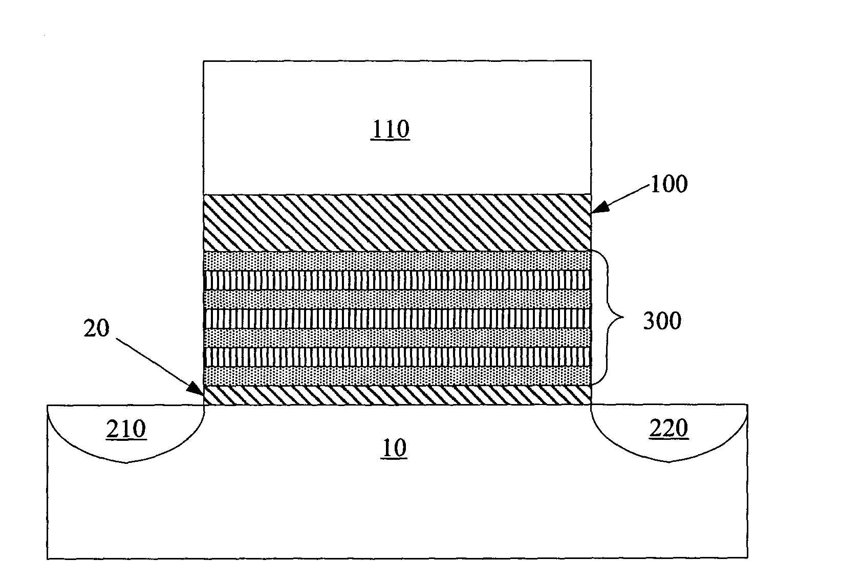
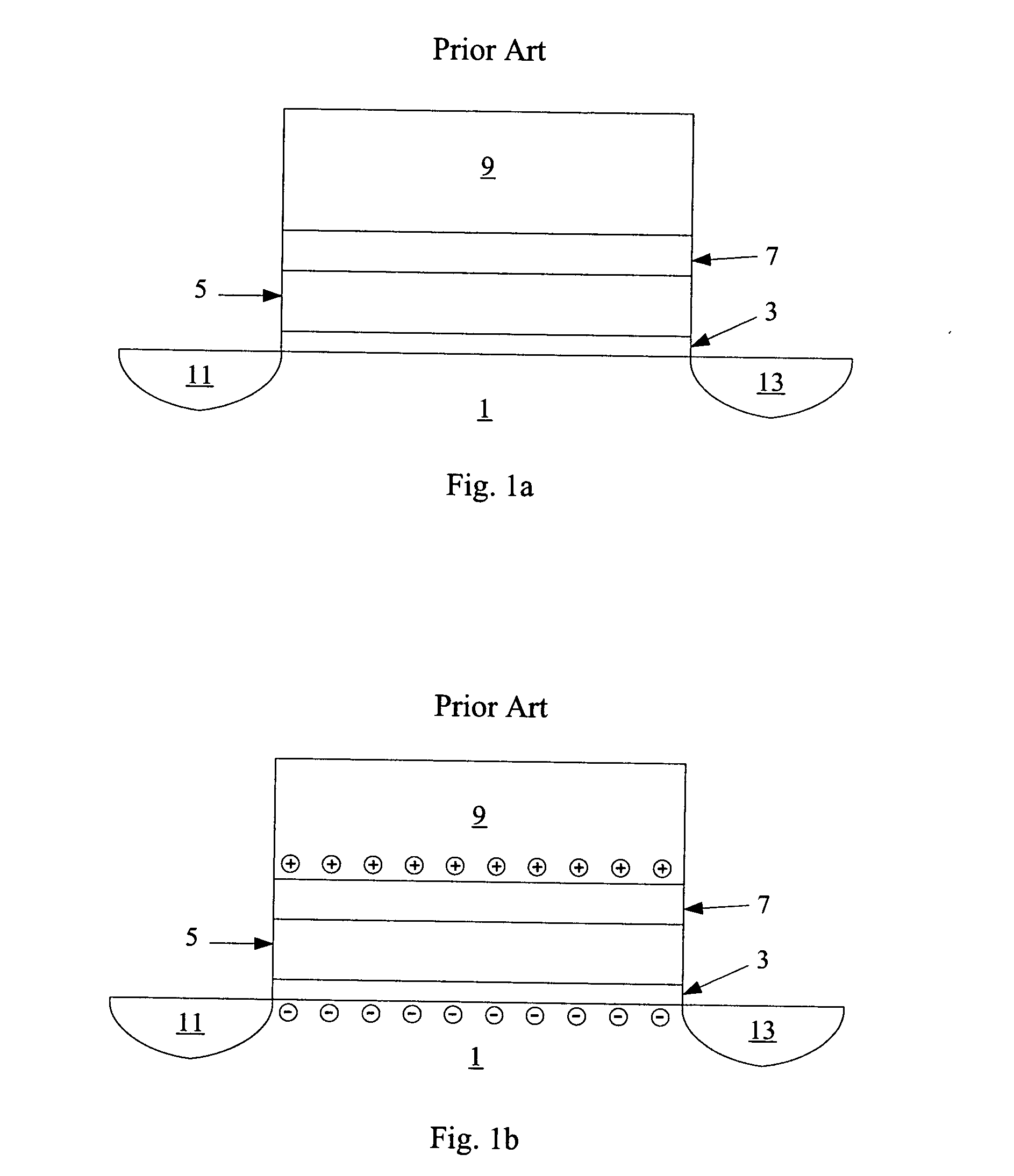
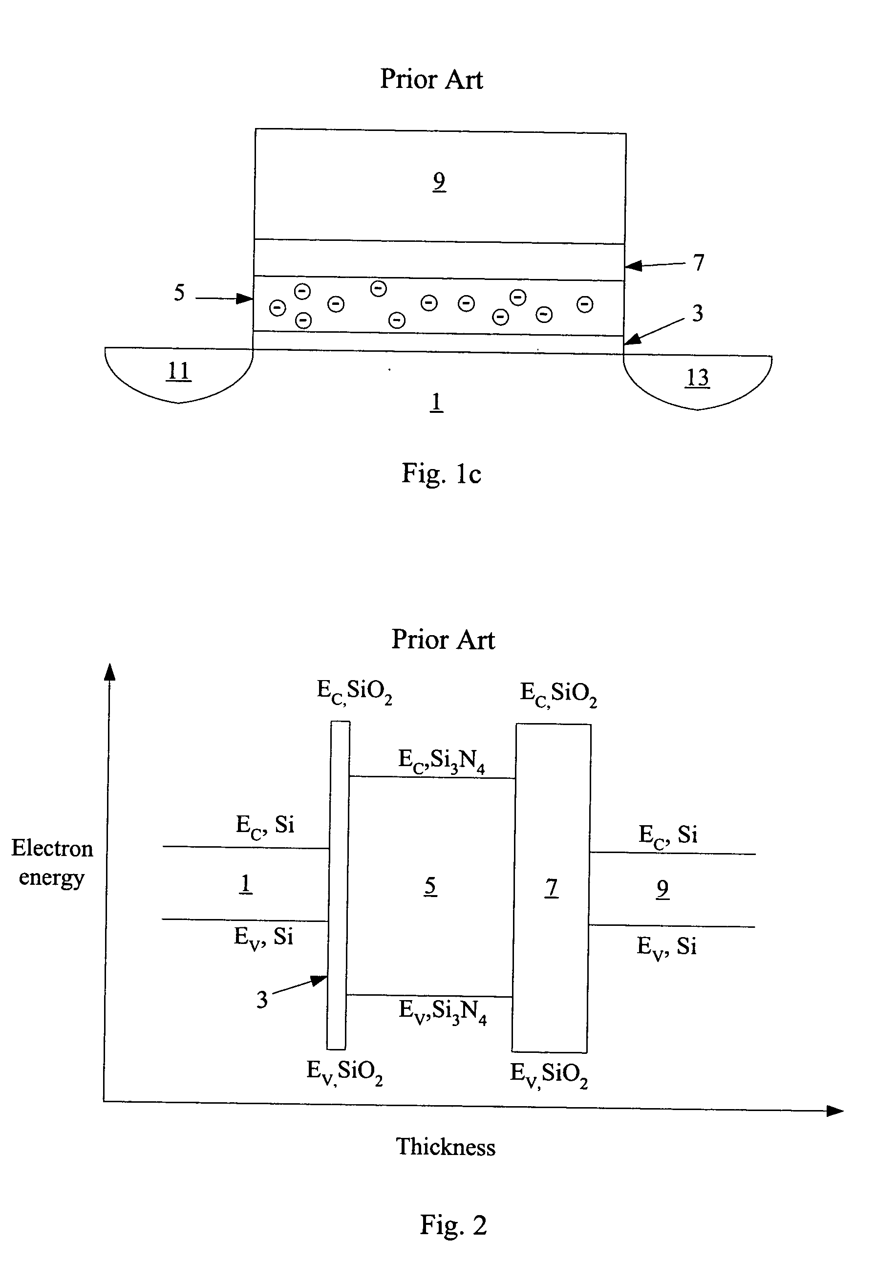
[0021] The present invention is an improved nonvolatile charge-storage memory cell related to a traditional SONOS device. A SONOS device, as shown in FIG. 1a, is a field effect transistor that operates as a nonvolatile memory cell by storing charge. A typical SONOS device is formed on a substrate 1 (conventionally a monocrystalline silicon wafer), upon which is formed a tunneling oxide 3 (normally silicon dioxide), a charge storage layer 5 (normally silicon nitride), a blocking oxide 7 (normally silicon dioxide), and a gate electrode 9 (typically of polycrystalline silicon, herein called polysilicon.) The silicon-oxide-nitride-oxide-silicon stack of substrate 1, tunneling oxide 3, charge storage layer 5, blocking oxide 7, and gate electrode 9 gives the SONOS device its name. Source region 11 and drain region 13 are formed in the substrate, for example by ion implantation.

[0022] Turning to FIG. 1b, in normal operation of, for example, a NMOS device, a positive charge is applied to g...


PUM

PropertyMeasurementUnit
dielectric constantaaaaaaaaaa
thickaaaaaaaaaa
thickaaaaaaaaaa

Abstract

The traditional nitride-only charge storage layer of a SONOS device is replaced by a multifilm charge storage layer comprising more than one dielectric material. Examples of such a multifilm charge storage layer are alternating layers of silicon nitride and silicon dioxide, or alternating layers of silicon nitride and aluminum oxide. The use of more than one material introduces additional barriers to migration of charge carriers within the charge storage layer, and improves both endurance and retention of a SONOS-type memory cell comprising such a charge storage layer.

Description

BACKGROUND OF THE INVENTION [0001] One conventional type of nonvolatile memory cell is a SONOS device, which operates by trapping charge in a charge storage layer. The presence or absence of stored charge distinguishes a programmed cell from an unprogrammed cell. [0002] Thus the ability of the cell to retain stored charge is crucial to its performance as a memory device. Stored charge tends to be lost from the cell over time and with successive write-erase cycles. [0003] Attempts have been made to improve retention of charge by optimizing the characteristics of nitride (the material most frequently used for the charge storage layer), using oxynitride used instead of nitride, applying heat treatments to nitride, etc. [0004] Some of these methods have shown some benefit, but there is a need to further improve retention and endurance of SONOS-type devices. SUMMARY OF THE INVENTION [0005] The present invention is defined by the following claims, and nothing in this section should be tak...

Claims


Application Information

Patent Timeline
Patent Type & Authority Applications(United States)
IPC IPC(8): H01L21/28H01L29/51H01L29/792
CPCH01L21/28185H01L21/28194H01L21/28202H01L29/792H01L29/513H01L29/517H01L29/518H01L21/28211
Inventor MAHAJANI, MAITREYEEWALKER, ANDREW J.CHEN, EN-HSING
Owner SANDISK TECH LLC
Why Eureka
Try Eureka