Lateral short-channel dmos, method of manufacturing the same, and semiconductor device

a technology of short-channel dmos and manufacturing methods, applied in the direction of semiconductor devices, electrical equipment, basic electric elements, etc., can solve the problems of high resistance, achieve low resistance, reduce resistance, and stabilize breakdown characteristics

Inactive Publication Date: 2005-03-24
SHINDENGEN ELECTRIC MFG CO LTD
View PDF7 Cites 32 Cited by
  • Summary
  • Abstract
  • Description
  • Claims
  • Application Information

AI Technical Summary

Benefits of technology

[0035] By using this construction, the current from the first conductivity-type drain region to the first conductivity-type source region when the lateral short-channel DMOS is ON flows in a deeper part (the first conductivity-type semiconductor region) than the second conductivity-type diffused region and also flows in part of the first conductivity-type diffused region that has relatively low resistance, so that the ON resistance can be reduced further.
[0036] Also, during reverse bias, the depletion layer can extend easily from the PN junction formed by the first conductivity-type diffused region and the second conductivity-type diffused region, so that there is also the effect that the electric field is distributed further and the breakdown characteristics can be stabilized even further.

Problems solved by technology

However, with this lateral short-channel DMOS, in order to realize the almost completely depleted state for the substrate surface during reverse bias, the dopant concentration of the N−-type epitaxial layer 948 cannot be set very high, so that there has been the problem of the resistance being high while the lateral short-channel DMOS is ON.

Method used


Image

  • Lateral short-channel dmos, method of manufacturing the same, and semiconductor device
  • Lateral short-channel dmos, method of manufacturing the same, and semiconductor device
  • Lateral short-channel dmos, method of manufacturing the same, and semiconductor device

Examples


embodiment 1

[0081] Embodiment 1

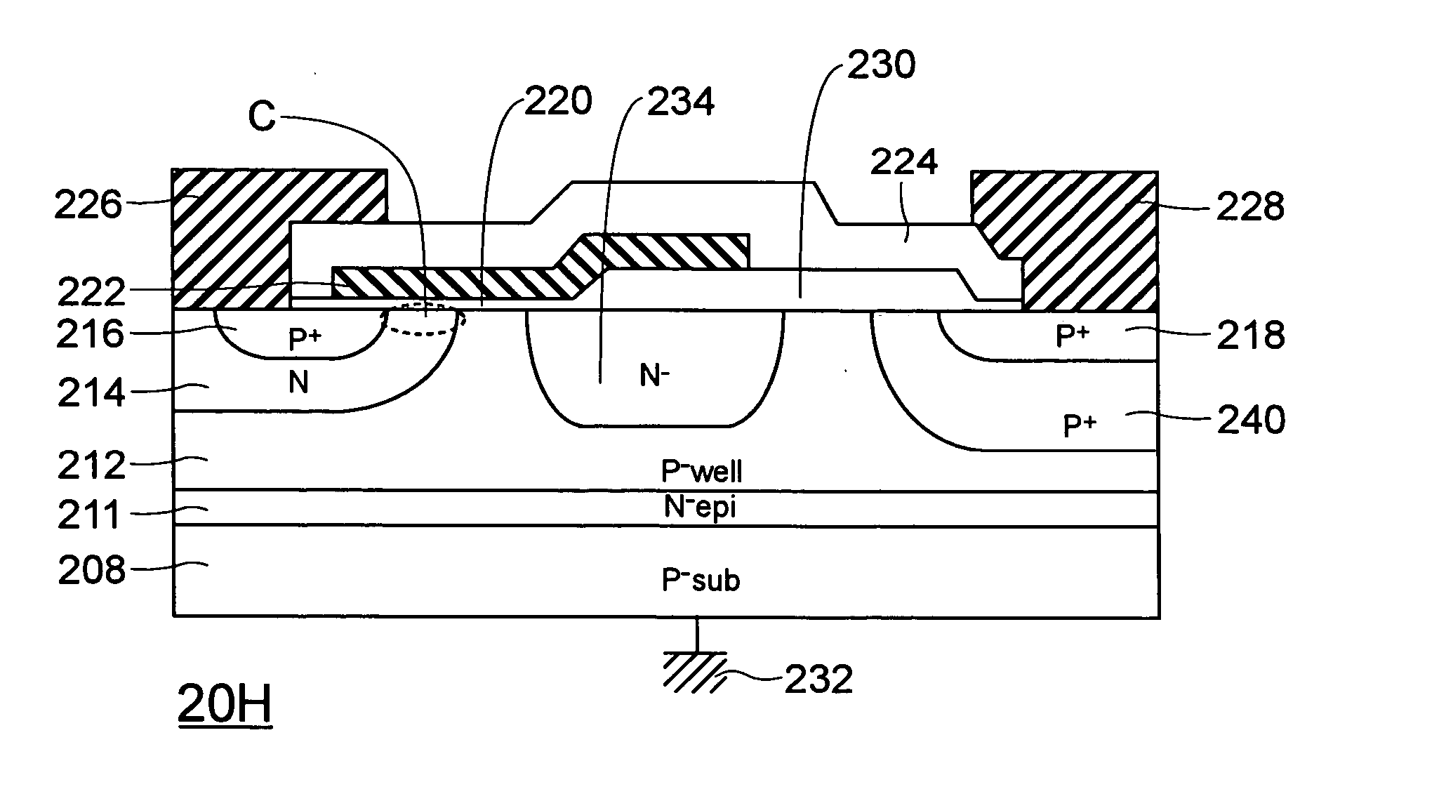
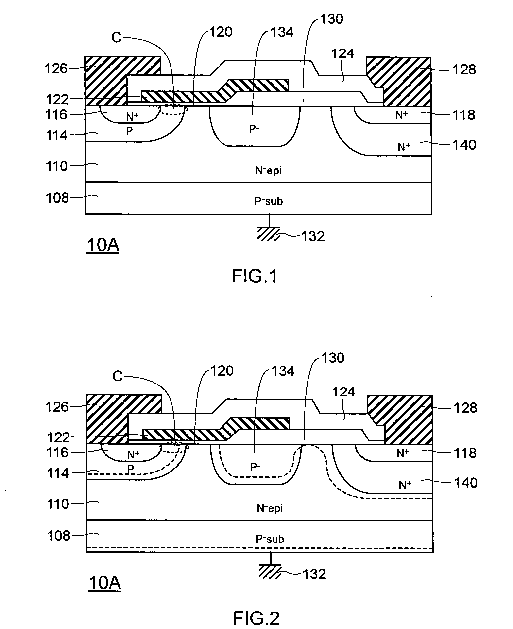
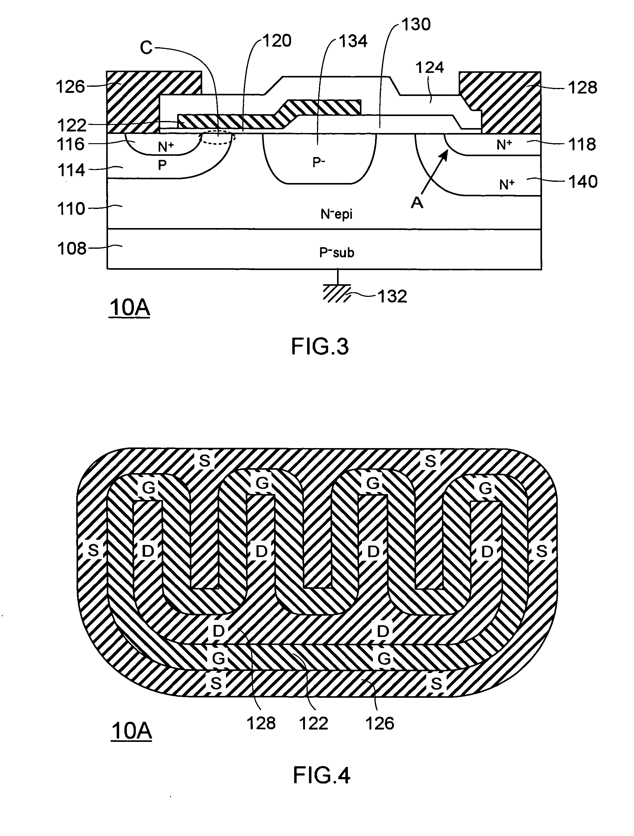
[0082]FIG. 1 is a cross-sectional view of a lateral short-channel DMOS according to Embodiment 1. FIGS. 2 and 3 are diagrams useful in explaining operational effects of the lateral short-channel DMOS according to Embodiment 1. FIG. 4 is a plan view of the lateral short-channel DMOS according to Embodiment 1.

[0083] As shown in FIG. 1, a lateral short-channel DMOS 10A according to Embodiment 1 has an N−-type epitaxial layer (first conductivity-type semiconductor region) 110 formed on one surface of a P−-type semiconductor substrate (semiconductor substrate) 108, and as shown in FIG. 2 is a so-called RESURF-type lateral short-channel DMOS in which the surface of the N−-type epitaxial layer 110 is almost completely depleted during reverse bias.

[0084] In this lateral short-channel DMOS 10A, a P-type well (second conductivity-type well) 114 including a channel forming region C is formed in the surface of the N−-type epitaxial layer 110, and an N+-source region (first ...

embodiment 2

[0098] Embodiment 2

[0099]FIG. 5 is a cross-sectional view of a lateral short-channel DMOS according to Embodiment 2. A lateral short-channel DMOS 10B according to Embodiment 2 has a similar structure to the lateral short-channel DMOS 10A according to Embodiment 1, but differs as shown in FIG. 5 in that an N−-type diffused region 136 including a higher concentration of N-type dopant than the N−-type epitaxial layer 110 is also formed in an N−-type epitaxial layer 110 surface side of the P−-type diffused region 134.

[0100] This means that according to the lateral short-channel DMOS 10B according to Embodiment 2, in addition to the effects of the lateral short-channel DMOS 10A according to Embodiment 1, the following effect is obtained. That is, the current from the N+-type drain region 118 to the N+-type source region 116 when the DMOS 10B is ON flows in a deeper part (the N−-type epitaxial layer 110) than the P−-type diffused region 134 and also flows in part of the N−-type diffused ...

embodiment 3

[0102] Embodiment 3

[0103]FIG. 6 is a cross-sectional view of a lateral short-channel DMOS according to Embodiment 3. A lateral short-channel DMOS 10C according to Embodiment 3 has a similar structure to the lateral short-channel DMOS 10B according to Embodiment 2, but differs as shown in FIG. 6 in that the N−-type diffused region 136 contacts the N+-type well 140.

[0104] According to the lateral short-channel DMOS 10C according to Embodiment 3, in addition to the effects of the lateral short-channel DMOS 10B according to Embodiment 2, the following effect is obtained. That is, the ON resistance of a current path from the N+-type well 140 to the N−-type diffused region 136 can be reduced further.


PUM


Abstract

A lateral short-channel DMOS according to the present invention is a lateral short-channel DMOS in which an N-type semiconductor region is formed, with the surface of the N-type semiconductor region becoming almost completely depleted during reverse bias. The lateral short-channel DMOS 10A according to the present invention includes an N-type epitaxial layer 110 that is formed in one surface of a P-type semiconductor substrate 108, a P-type well 114 that is formed in the surface of the N-type epitaxial layer 110 and includes a channel forming region C, an N+-type source region 116 that is formed in a surface of the P-type well 114, an N+-type drain region 118 formed in a surface of the N-type epitaxial layer 110, and a gate electrode 122 formed via a gate insulating film 120 in at least an upper part of the channel forming region C out of a region from the N+-type source region 116 to the N+-type drain region 118. The lateral short-channel DMOS 10A according to the present invention also includes an N+-type well 140 that is formed in a surface of the N-type epitaxial layer 110 and includes a higher concentration of N-type dopant than the N-type epitaxial layer 110 and a lower concentration of N-type dopant than the N+-type drain region 118, with the N+-type drain region 118 being formed in a surface of this N+-type well 140. As described above, according to the present invention, ON resistance is reduced while maintaining high breakdown characteristics, so that it is possible to provide a lateral short-channel DMOS with high breakdown characteristics and superior current driving characteristics.

Description

TECHNICAL FIELD [0001] The present invention relates to a lateral short-channel DMOS that can be favorably used as a power MOSFET and a method of manufacturing the same. The present invention also relates to a semiconductor device equipped with this lateral short-channel DMOS. RELATED ART [0002]FIG. 14 is a cross-sectional view of a conventional lateral short-channel DMOS disclosed in U.S. Pat. No. 4,866,495. FIG. 15 is a plan view of a semiconductor device including this lateral short-channel DMOS. In this lateral short-channel DMOS 90, an N−-type epitaxial layer 948 is formed on one surface of a P−-type semiconductor substrate 940. A P-type well including a channel forming region is then formed in a surface of the N−-type epitaxial layer 948, and N+-type source regions 956, 957 are formed in a surface of this P-type well. An N+-type drain region 970 is also formed in a surface of the N−-type epitaxial layer 948. Gate electrodes 963, 964 are then formed via gate insulating films 96...

Claims


Application Information

Patent Timeline
Patent Type & Authority Applications(United States)
IPC IPC(8): H01L21/336H01L29/06H01L29/08H01L29/10H01L29/417H01L29/76H01L29/78H01L29/94H01L31/062H01L31/113
CPCH01L29/0619H01L29/0634H01L29/0696H01L29/0878H01L29/7816H01L29/1095H01L29/4175H01L29/41758H01L29/66681H01L29/1083
Inventor KITAGUCHI, MAKOTO
Owner SHINDENGEN ELECTRIC MFG CO LTD
Why Eureka
Try Eureka