
Dynamically adjustable decoupling capacitance to reduce gate leakage current

a gate leakage current and capacitance technology, applied in the field of dynamically adjustable decoupling capacitance to reduce gate leakage current, can solve the problems of large switching current, high-speed integrated circuit devices that present many design challenges, and the need for very fast switching speeds, so as to reduce switching noise

Inactive Publication Date: 2005-03-24
TAIWAN SEMICON MFG CO LTD
View PDF5 Cites 28 Cited by
  • Summary
  • Abstract
  • Description
  • Claims
  • Application Information

AI Technical Summary

Benefits of technology

A principal object of the present invention is to provide an effective and very manufacturable method to reduce switching noise on an integrated circuit power supply.
A further object of the present invention is to reduce switching noise while limiting current leakage.
A yet further object of the present invention is to provide a method to reduce switching noise that is applicable to a variety of switchable capacitor arrangements.
Another further object of the present invention is to provide an integrated circuit device with reduced switching noise on the power supply.
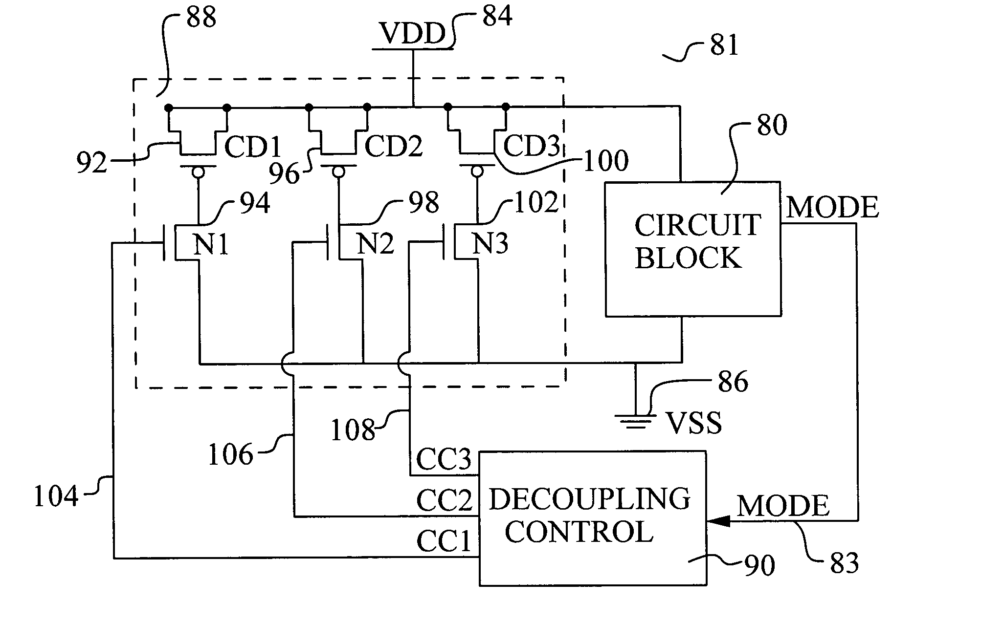
In accordance with the objects of this invention, a method to reduce switching noise on an integrated circuit device is achieved. The method comprises providing an integrated circuit device comprising a power supply, a ground, and a plurality of switchable capacitors. Each switchable capacitor is connected from the power supply to ground. The operating mode of the integrated circuit device is tracked. An optimal capacitance value is selected based on the operating mode. A set of switchable capacitors from the plurality of switchable capacitors is selected to thereby connect the optimal capacitance value from the power supply to ground.

Problems solved by technology

Very high-speed integrated circuit devices present many design challenges.
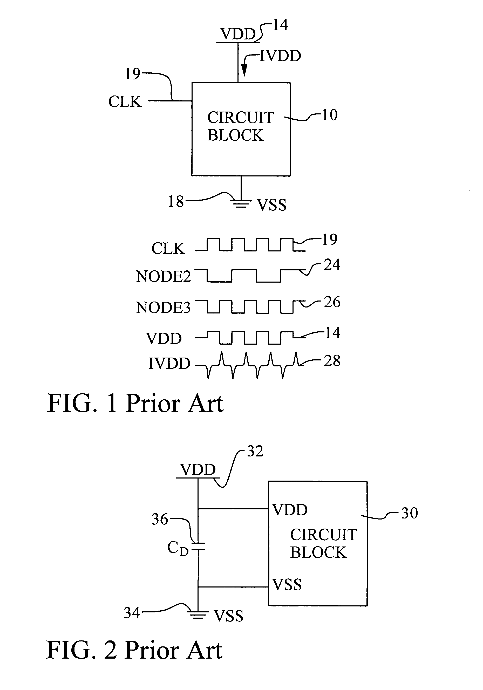
For example, synchronized switching of a large number of circuits, as with a very high-speed clock, can create very large switching currents.
In addition, if a very high-speed clock frequency is used, then the switching speeds must be very fast.
These large switching currents can cause a substantial amount of switching noise to be coupled onto the VDD line14 as shown.
A large switching noise can cause the circuit 10 to malfunction at such a low operating voltage level.
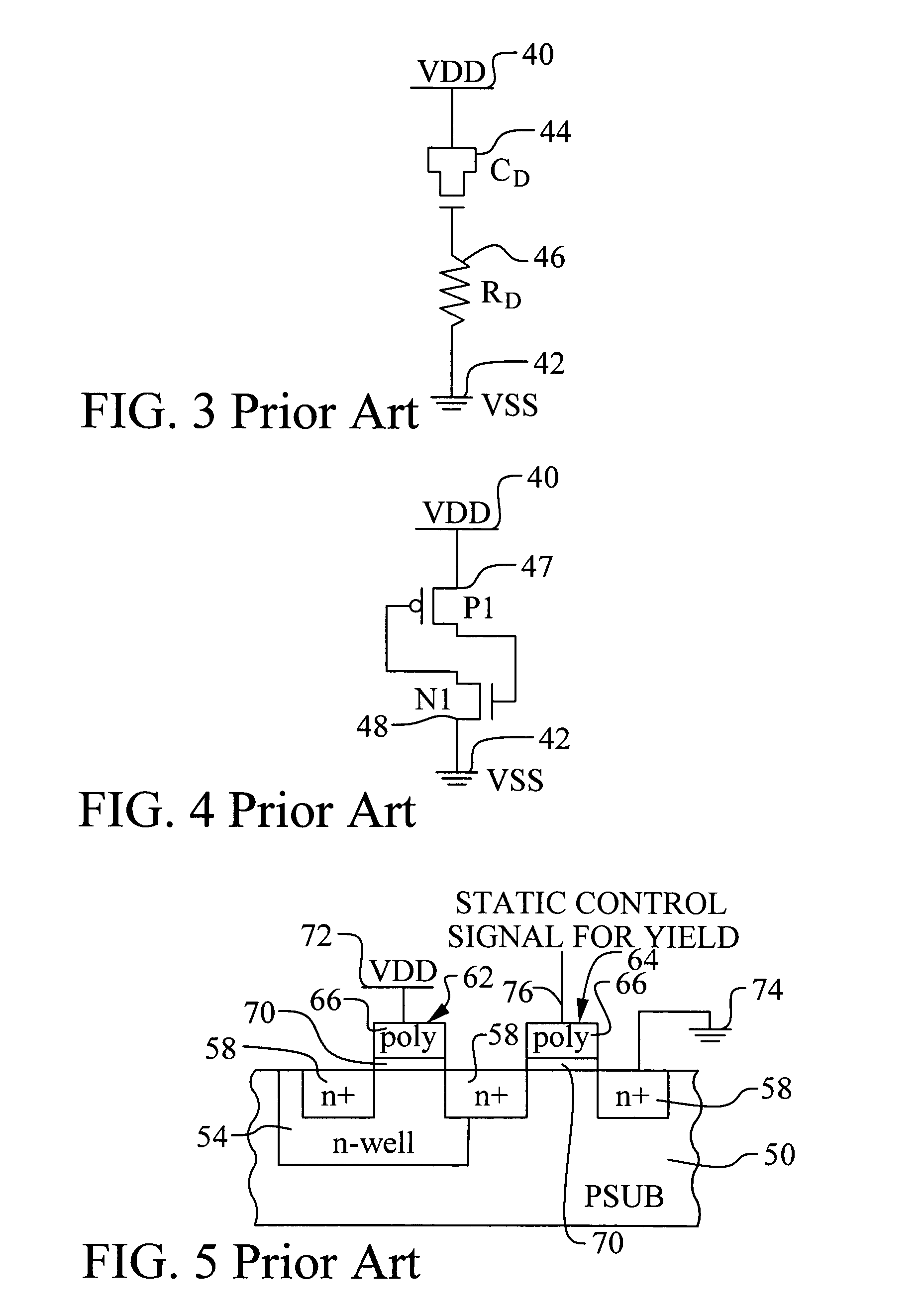
It is observed in the art that, as process technology shrinks to sub-0.13 micron, MOS gate leakage current becomes a serious problem.
Unfortunately, when very large decoupling capacitors 62 are formed using MOS gates, the large gate leakage can cause an unacceptable current drain on the circuit.
In addition, the large gate area of the decoupling capacitors 62 is a likely location for a gate defect that can cause the capacitor to be shorted.
If a decoupling capacitor fails, then a fuse is blown to disable a grounding switch.

Method used


Image

  • Dynamically adjustable decoupling capacitance to reduce gate leakage current
  • Dynamically adjustable decoupling capacitance to reduce gate leakage current
  • Dynamically adjustable decoupling capacitance to reduce gate leakage current

Examples


Embodiment Construction

The preferred embodiments of the present invention disclose a method to reduce switching noise in a power supply of an integrated circuit device. A method to dynamically adjust decoupling capacitance is disclosed. A device is described wherein dynamic adjustment of decoupling capacitance is achieved. It should be clear to those experienced in the art that the present invention can be applied and extended without deviating from the scope of the present invention.

Referring now to FIG. 6, a first preferred embodiment of the present invention is illustrated. Several important features of the present invention are shown and discussed below. In the first embodiment, an integrated circuit 81 first comprises a circuit block 80. The circuit block 80 preferably comprises a plurality of logic circuits capable of switching digital states. The circuit block 80 may be the entire logic section of the integrated circuit 81 or may be only one of several blocks. In the case of multiple sections or...


PUM


Abstract

A new method to reduce switching noise on an integrated circuit device is achieved. The method comprises providing an integrated circuit device comprising a power supply, a ground, and a plurality of switchable capacitors. Each switchable capacitor is connected from the power supply to ground. The operating mode of the integrated circuit device is tracked. An optimal capacitance value is selected based on the operating mode. A set of switchable capacitors from the plurality of switchable capacitors is selected to thereby connect the optimal capacitance value from the power supply to ground.

Description

BACKGROUND OF THE INVENTION (1) Field of the Invention The invention relates to an integrated circuit device, and, more particularly, to a method to decouple switching current noise from a power supply of an integrated circuit device. (2) Description of the Prior Art Very high-speed integrated circuit devices present many design challenges. For example, synchronized switching of a large number of circuits, as with a very high-speed clock, can create very large switching currents. Referring now to FIG. 1, an exemplary integrated circuit block 10 is illustrated. The circuit block 10 is connected to power supply VDD 14 and ground 18. The circuit block 10 comprises a large number of logic circuits capable of very high-speed operation. During normal operation, internal circuit nodes, such as NODE224 and NODE326 will switch states as synchronized by the system clock CLK 19. At any time, a large number of nodes may be switching. In addition, if a very high-speed clock frequency is used...

Claims


Application Information

Patent Timeline
IPC IPC(8): H03B1/00
CPCH03J2200/10H03J1/0008
Inventor WANG, WEN-TAIHU, CHANG-FEN
Owner TAIWAN SEMICON MFG CO LTD
Learn More