Drift-sensitive laser trimming of circuit elements

Inactive Publication Date: 2005-03-24
GSI LUMONICS CORP
View PDF21 Cites 26 Cited by
  • Summary
  • Abstract
  • Description
  • Claims
  • Application Information

AI Technical Summary

Benefits of technology

[0056] One embodiment of the present invention provides a method for laser trimming a circuit element. The method includes identifying parameters associated with the element that are substantial contributors to subsequent drift in element value. The identified parameters include, for example, at least one of a paste composition from which the element is formed, a subsequent manufacture processing step to which the element is subject

Problems solved by technology

However, each resistor element 120, as applied to or formed onto the ceramic substrate 110 may have a resistance value that falls outside of the desired range due to uncontrollable aspects of forming the resistive elements onto the substrate.
In addition, the cost of fabricating embedded resistors is lower than the cost of separately fabricating and then surface mounting surface mount resistors.
A significant problem with the use of embedded passive elements is that the electrical characteristics of the deposited or etched elements are difficult to control and predict because of variables in the fabrication process.
For many applications, it has not been possible to fabricate embedded elements with sufficient accuracy due to these limitations.
This has limited the use of embedded passive printed circuit boards in many critical performance systems.
The majority of the problems associated with embedding resistors within layers of a PCB panel relate to the typical materials used for the resistor elements, the substrate or mounting material, and any surrounding materials proximate to the resistor such as a dielectric layer laminated or coated on top of the resistor.
Thickness and composition of the resistive layer are susceptible to variation due to difficulty in control of the process parameters used to deposit the film.
During these cycles, one or more pastes will have more than one curing cycle, making the prediction of final resistance values for these resistors quite complex.
Furthermore, the low temperature and short time used for the curing process result in a cured paste that is softer and less temperature stable than its high temperature counterpart.
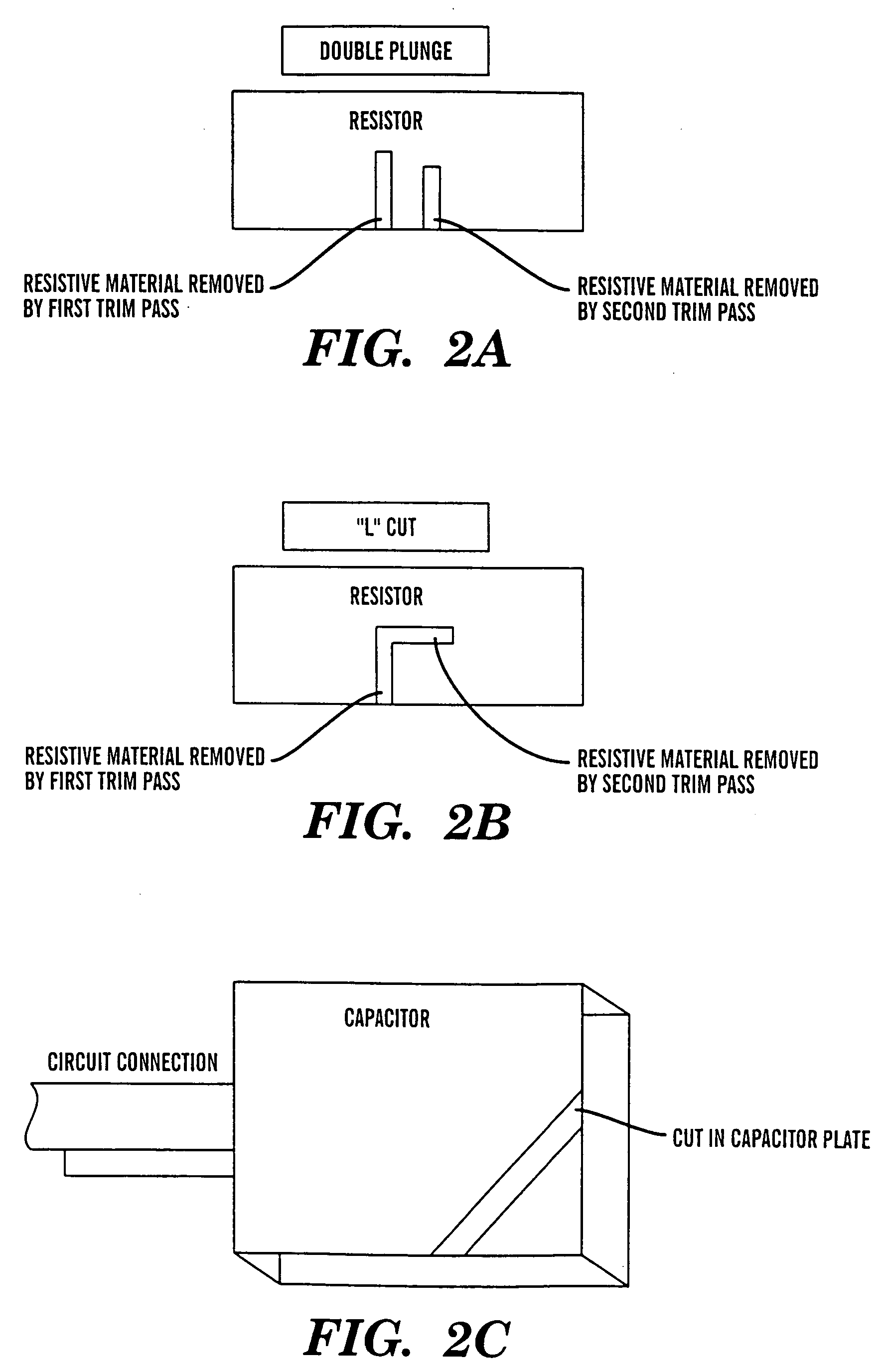
This profile may result f

Method used


Image

  • Drift-sensitive laser trimming of circuit elements
  • Drift-sensitive laser trimming of circuit elements
  • Drift-sensitive laser trimming of circuit elements

Examples


case 5

[0163] Case 5 is a particularly interesting example of an implementation in which no drift is allowed after lamination. As shown, initial indications are that untrimmed resistors have negative drift of about 4% after lamination. Laser trimmed resistors have positive, e.g. 4% to 8%, post-lamination drift. Thus, by choosing the correct trimming parameters the final drift can be reduced to substantially 0%.

[0164] It will be recognized that the trimming may be performed in multiple phases. That is, all passive elements may first be subjected to a rough trimming and then be subjected to a fine trimming after the rough trimmed elements have cooled.

[0165] Following determination of trim (cut) speed (bite size, spot size, and repetition rate) in step 1615, operations continue with FIG. 17. In step 1701 the position of the element in relation to the any conductors (copper traces) is determined. Typically this is done by doing a global alignment (3 or 4 point alignment) to determine where th...


PUM

PropertyMeasurementUnit
Dielectric polarization enthalpyaaaaaaaaaa
Electrical resistanceaaaaaaaaaa
Electrical conductoraaaaaaaaaa

Abstract

In the laser trimming of passive circuit elements such as resistors, capacitors and inductors, various trimming parameters must be selected. To select a parameter, such as a cut type or speed, a value of a parameter, such as the resistance or impedance of a resistor, of each of a plurality of elements is measured. The measured parameter value of each element is compared with a target value for the parameter to determine an offset value between the measured parameter value and the target value. The relevant trim parameters are then selected based on the determined offset values.

Description

RELATED APPLICATIONS [0001] This application is a continuation of U.S. application Ser. No. 10 / 103,317, filed Mar. 22, 2002, which is herein incorporated in its entirety by reference.FIELD OF THE INVENTION [0002] The present invention relates to trimming elements formed on a panel or other work piece. More particularly the present invention relates to trimming elements, such as resistors, capacitors or other passive circuit elements, which may be later embedded in a layer of a multi-layer work piece, such as a printed circuit board (PCB). BACKGROUND OF THE INVENTION [0003] Material processing is used to adjust the performance of electronic elements by removing or otherwise affecting a portion of the material of the electronic element to change the electrical characteristics thereof. It is known to change the electrical properties of passive and some active electronic elements by removing material therefrom. Methods of removing material include applying laser energy for vaporizing a ...

Claims


Application Information

Patent Timeline
IPC IPC(8): B23K26/00H01C17/242H05K1/16
CPCB23K26/0003H05K1/16H01C17/242B23K26/351
Inventor NAUMOV, ANDREIKITAI, ANTONMILLER, IAN J.
Owner GSI LUMONICS CORP
Why Eureka
Try Eureka