

Depletion drain-extended MOS transistors and methods for making the same
a technology of drainextension and mos transistor, which is applied in the direction of semiconductor devices, basic electric elements, electrical equipment, etc., can solve the problems of poor breakdown voltage rating of devices, unsuitable operation of conventional depletion mos devices, etc., and achieves convenient operation, safe device operation, and mitigate current flow constriction
- Summary
- Abstract
- Description
- Claims
- Application Information
AI Technical Summary
Benefits of technology
Problems solved by technology
Method used
Image

Examples
Embodiment Construction
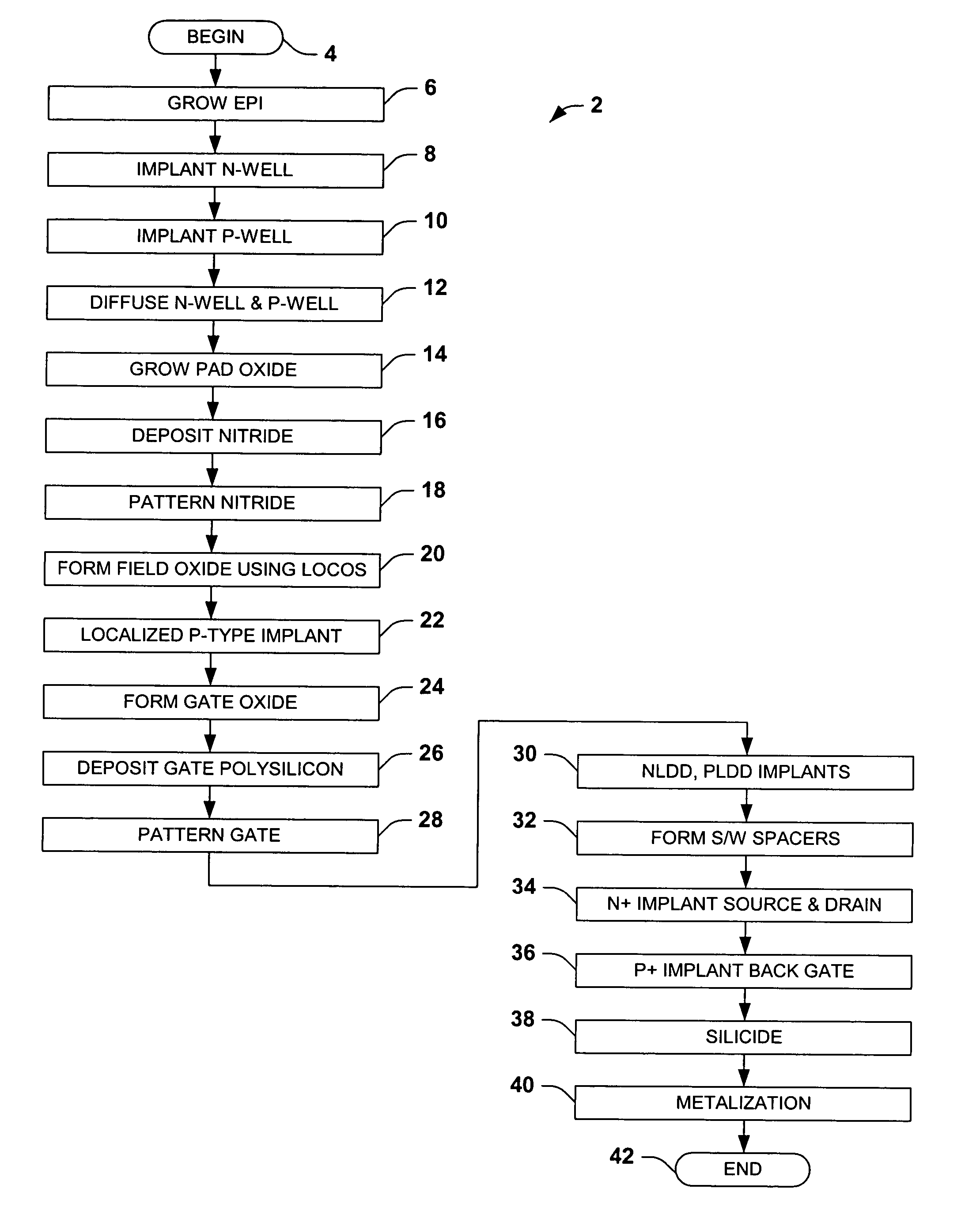
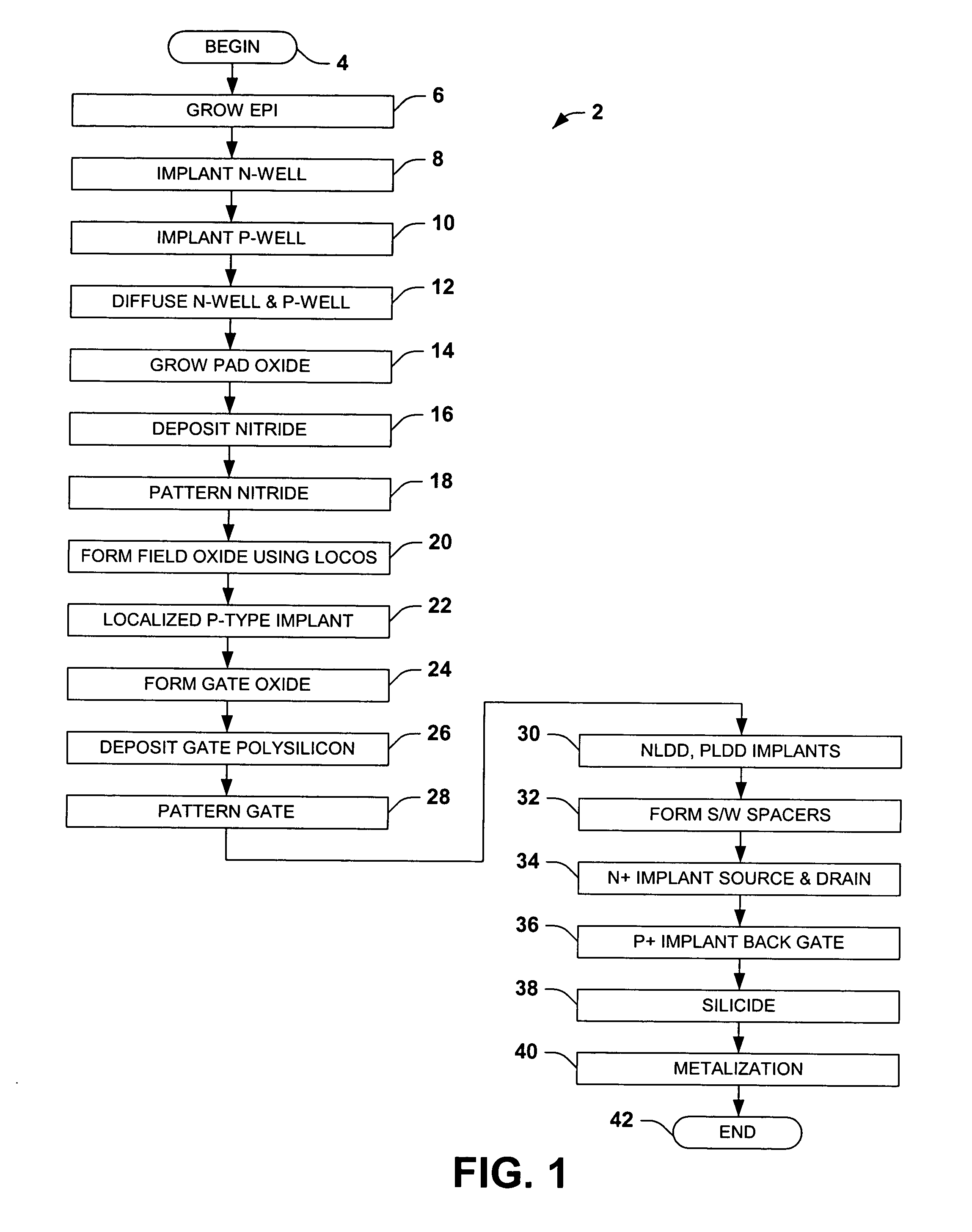
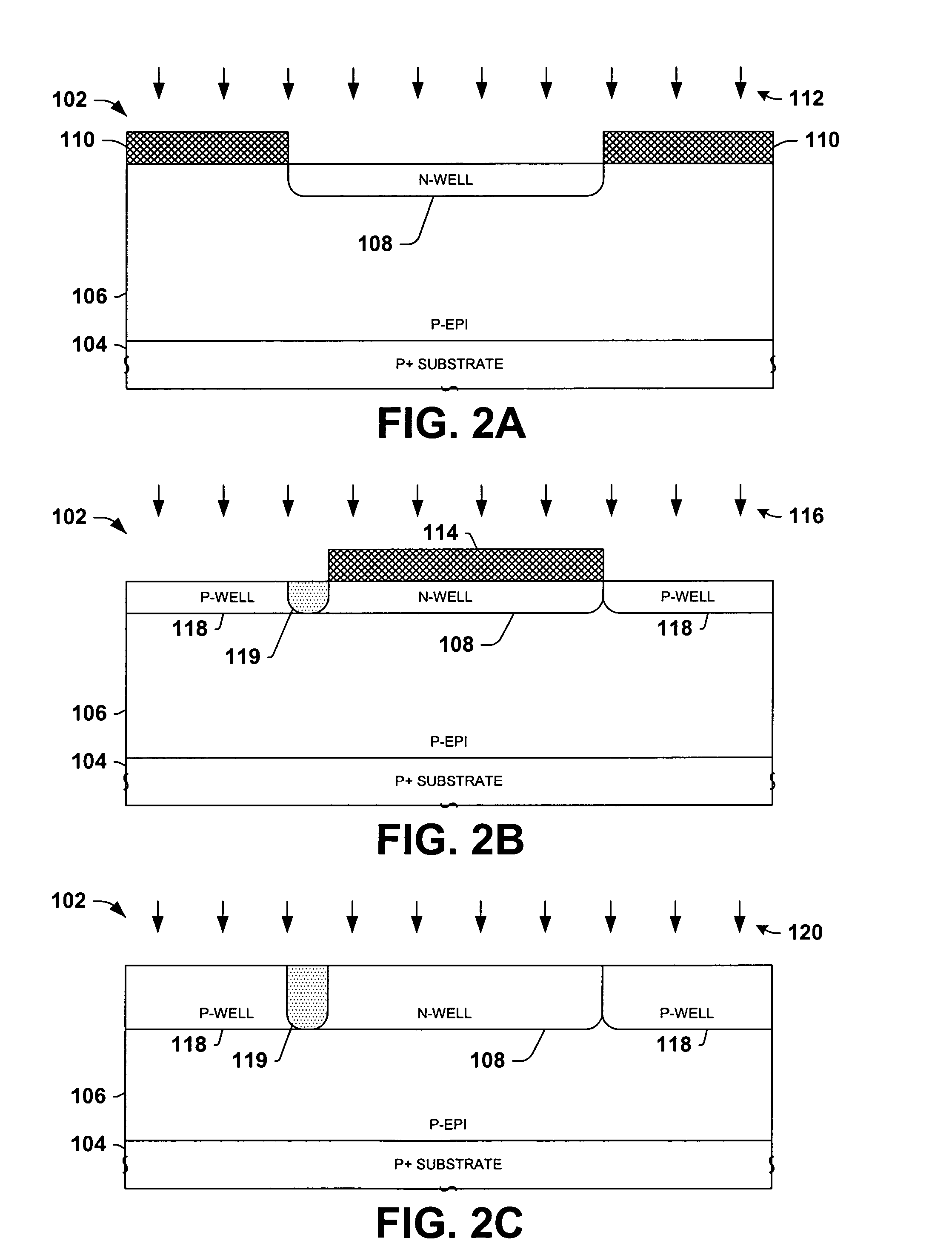
[0022] One or more implementations of the present invention will now be described with reference to the attached drawings, wherein like reference numerals are used to refer to like elements throughout. The invention relates to depletion drain-extended MOS transistors and fabrication methods, wherein a compensated channel region is provided with p and n type dopants for depletion operation. An adjust region is provided in the substrate proximate a channel side end of a thick gate dielectric structure to facilitate high voltage operation with improved breakdown voltage performance and to inhibit CHC degradation. Although illustrated and described below in the context of n-channel devices (DENMOS transistors), the invention may also be employed in association with PMOS transistors. Furthermore, while the invention is illustrated and described with respect to DENMOS transistors fabricated using p-type silicon substrates with a p-type epitaxial layer formed thereover, the invention is no...
PUM
 Abstract
Description
Claims
Application Information