Method for interlayer and yield based optical proximity correction

a yield-based, optical proximity correction technology, applied in the field of semiconductor fabrication, can solve the problems of difficult calculation of exact correction values, limited pattern fidelity of process, and general belief in limited usefulness of non-iterative rules based opc, so as to improve the optical proximity correction process, improve the lithographic processing of integrated circuits, and improve the effect of optical proximity correction

Inactive Publication Date: 2005-03-24
GLOBALFOUNDRIES INC
View PDF17 Cites 39 Cited by
  • Summary
  • Abstract
  • Description
  • Claims
  • Application Information

AI Technical Summary

Benefits of technology

[0013] It is, therefore, an object of the present invention to provide an improved lithographic processing of integrated circuits

Problems solved by technology

However, this process is not only limited in its pattern fidelity due to the small size of the patterns being printed relative to the wavelength of the light used, but it is also limited by a variety of other nonlinear effects involved in the overall process.
While proven to be efficient at correcting some important one- and two-dimensional imaging problems, non-iterative rules based OPC is generally believed limited in its usefulness due to the finite number of rules that are available to describe all layout situations, the diff

Method used


Image

  • Method for interlayer and yield based optical proximity correction
  • Method for interlayer and yield based optical proximity correction
  • Method for interlayer and yield based optical proximity correction

Examples


Embodiment Construction

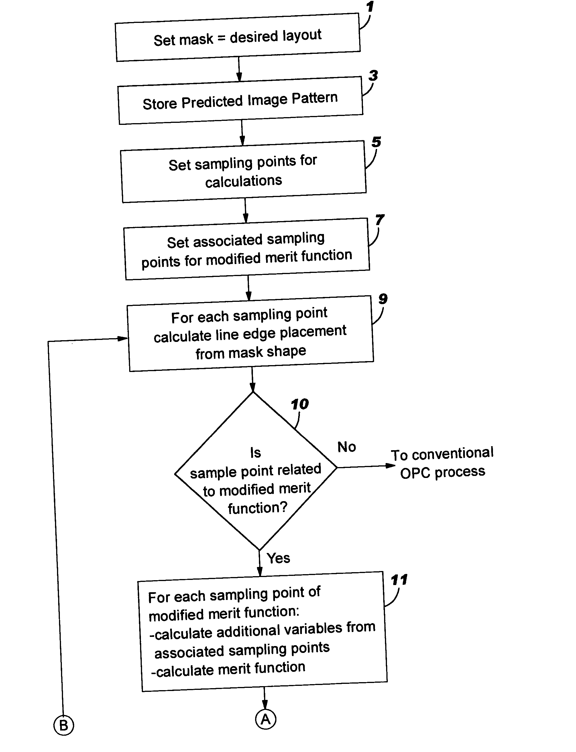
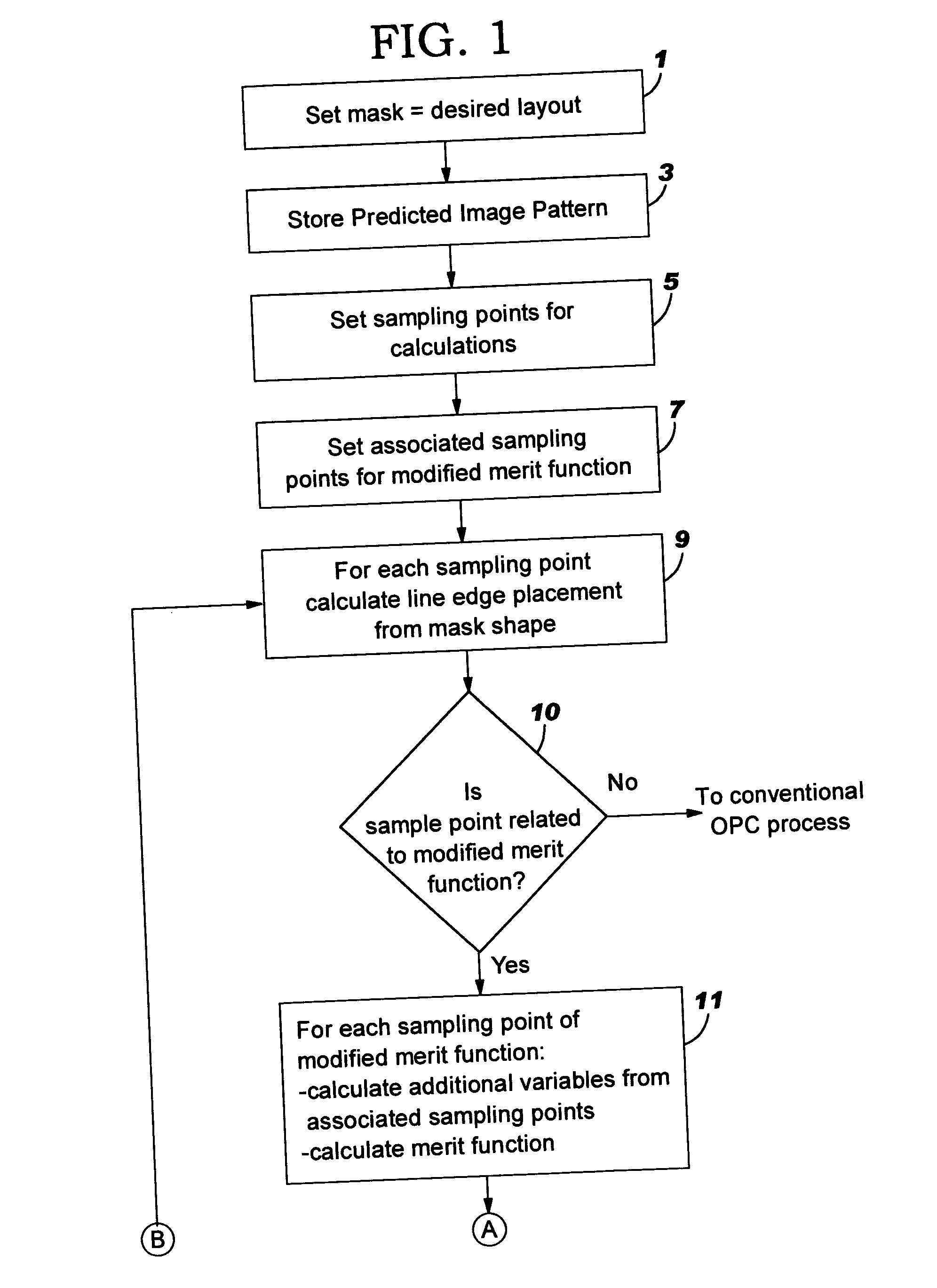
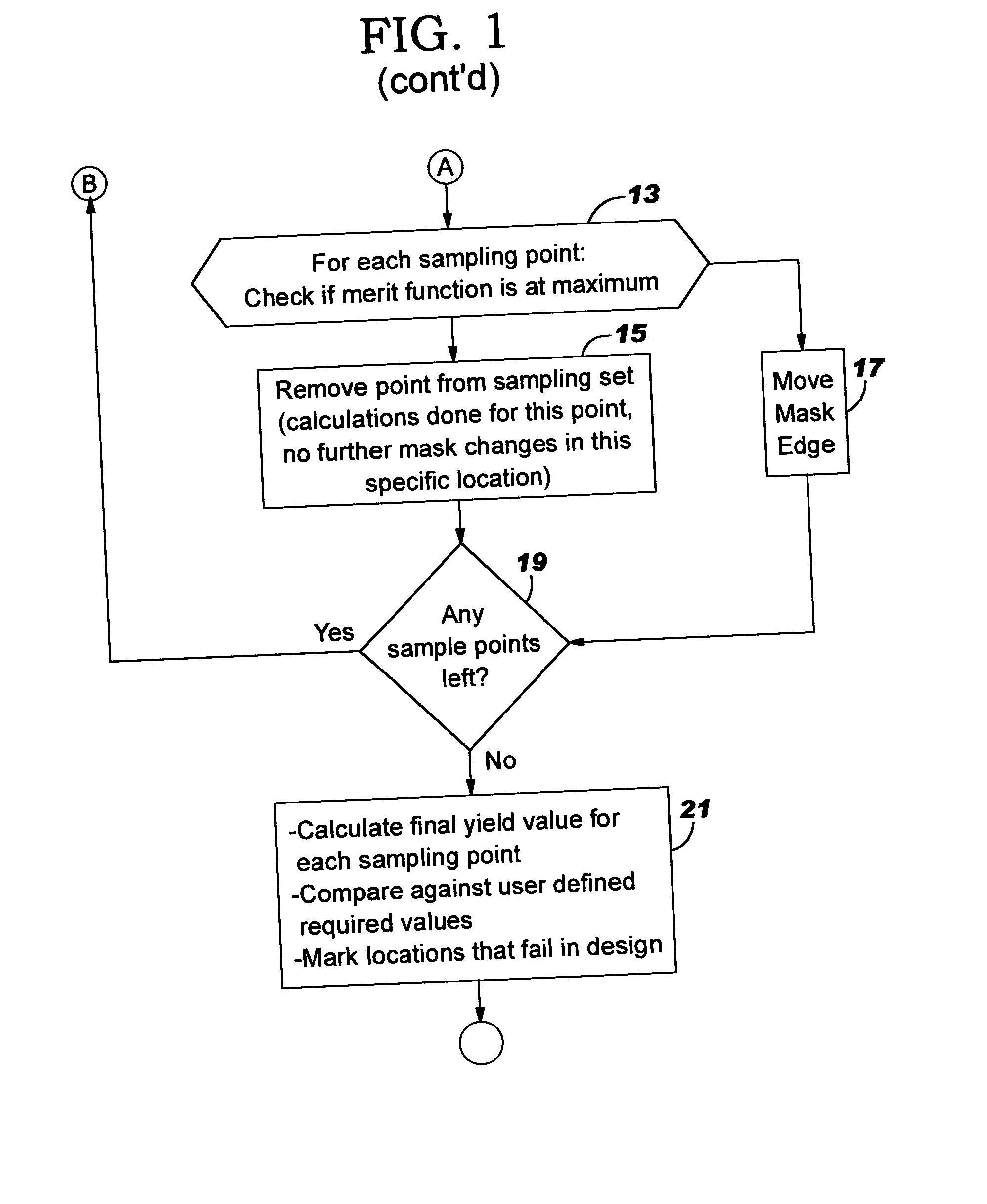
[0029] With reference to FIG. 1, there is shown a flow chart embodying one possible manner in which a conventional model-based OPC process may be modified, in accordance with the present invention, to implement a yield based process that converges on an optimum layout rather than on the original design layout.

[0030] In this regard, conventional model-based OPC tools optimize to the original design layout by the iterative process of comparing a predicted wafer image to the design layout. To achieve this, the actual circuit pattern design layout to be reproduced on a substrate layer is created on a mask. An existing OPC tool then runs a simulation on this pattern and predicts the actual wafer pattern image that would be transmitted onto the wafer substrate, taking into consideration optical proximity effects, and the like. The OPC tool then compares this predicted wafer image with the original circuit design layout, determines the required adjustment of the mask pattern so that the m...


PUM


Abstract

An optical proximity correction method is provided using a modified merit function based upon yield. Known failure mechanisms related to layout geometries are used to derive yield functions based upon distance values between layout features, such as, edge features. In comparing the edge points on the predicted layout pattern with the corresponding point on the design layout pattern, a yield test is first undertaken before movement of the points on the predicted layout pattern to a position of higher yield. Where yield is acceptable, no further movement is made. Where incremental movement of points results in coming within acceptable proximity before acceptable yield is reached, the point is flagged for further consideration.

Description

BACKGROUND OF THE INVENTION [0001] 1. Field of the Invention [0002] The present invention relates to semiconductor fabrication and, more particularly, to an improved method for creating mask patterns for use in lithographic processing of integrated circuits (ICs). [0003] 2. Background and Related Art [0004] Integrated circuits are fabricated by lithographic techniques where energy beams transmit integrated circuit images or patterns on photomasks onto photosensitive resists on semiconductor wafer substrates. This lithographic transfer of mask patterns into photoresist, development of the photoresist, followed either by ion implant or etch processes is a standard process for creating chips. However, this process is not only limited in its pattern fidelity due to the small size of the patterns being printed relative to the wavelength of the light used, but it is also limited by a variety of other nonlinear effects involved in the overall process. Thus, in addition to the limited resol...

Claims


Application Information

Patent Timeline
IPC IPC(8): G03F1/14G03F1/08G06F17/50H01L21/027
CPCG03F1/144G03F7/70441G03F1/36
Inventor ZACH, FRANZ XAVER
Owner GLOBALFOUNDRIES INC
Why Eureka
Try Eureka