Deposition of silicon-containing films from hexachlorodisilane

a technology of hexachlorodisilane and silicon-containing films, which is applied in the direction of chemically reactive gases, crystal growth processes, polycrystalline material growth, etc., can solve the problems of non-selective (blanket) and selective deposition of silicon-containing films for future devices, and the deposition selectivity of traditional silane and dichlorosilane source gas processes is limited with respect to different substrate materials

Inactive Publication Date: 2005-03-31
TOKYO ELECTRON LTD
View PDF8 Cites 69 Cited by
  • Summary
  • Abstract
  • Description
  • Claims
  • Application Information

AI Technical Summary

Benefits of technology

[0005] An object of the present invention is to provide a method and system for deposition of silicon-containing films on a semiconductor wafer in a process chamber of a processing system which reduces or solves the above described and / or other problems with prior art deposition systems and methods.

Problems solved by technology

Moreover, it is evident that non-selective (blanket) and selective deposition of silicon-containing films will be needed for future devices.
Moreover, the traditional silane and dichlorosilane source gas processes have limited deposition selectivity with respect to different substrate materials.

Method used


Image

  • Deposition of silicon-containing films from hexachlorodisilane
  • Deposition of silicon-containing films from hexachlorodisilane
  • Deposition of silicon-containing films from hexachlorodisilane

Examples


Embodiment Construction

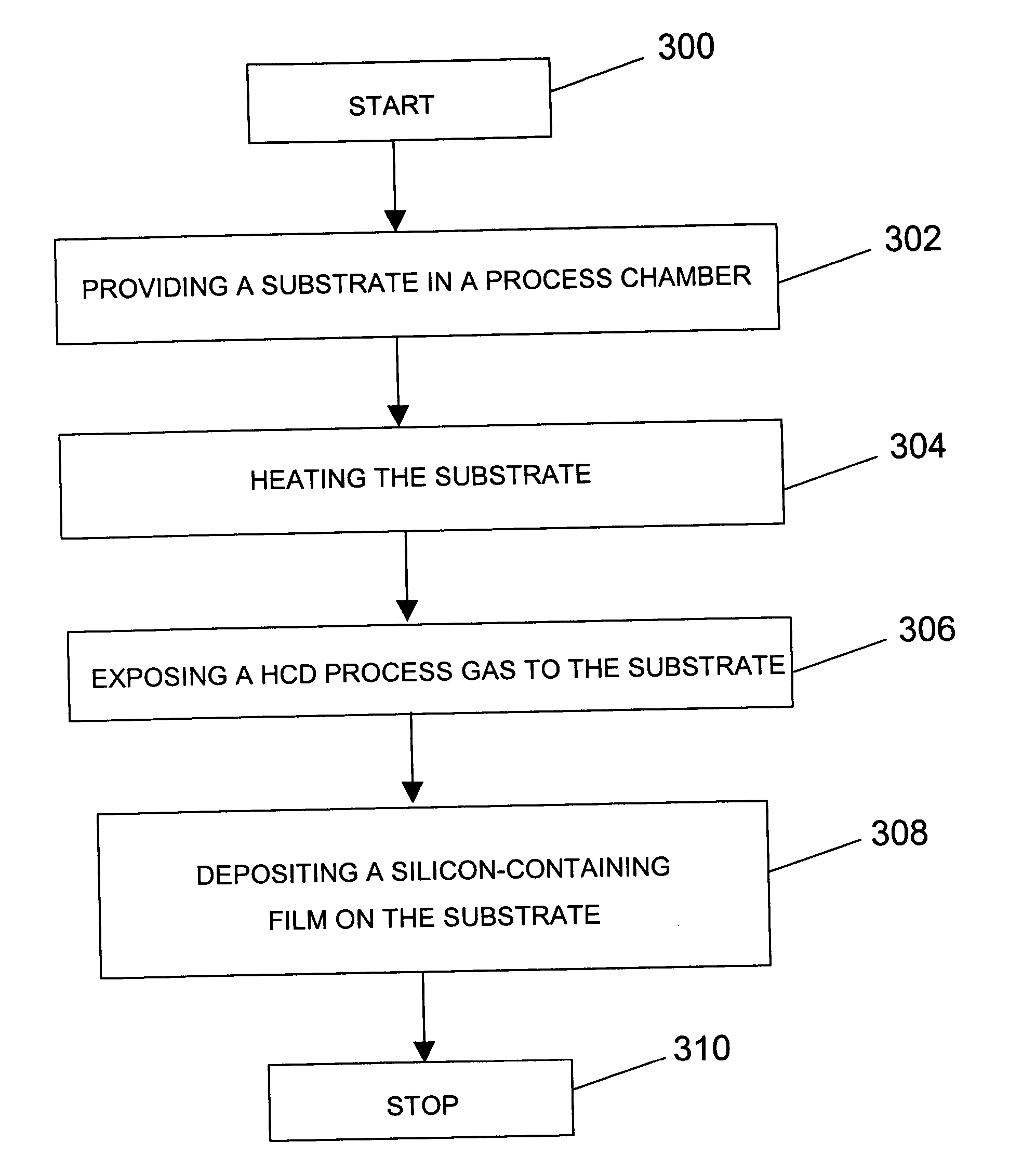
[0023] As noted in the Background of the Invention section above, the use of traditional silicon source gases will not provide low temperature deposition of silicon-containing films or sufficient selectivity of the film growth. Nevertheless, use of other silicon source gases has gone largely unstudied, perhaps due to the difficulty of implementing new source gases in the semiconductor industry and the problem of providing uniform process results at different wafer positions in a batch type process chamber. Thus, the present inventors have conducted experiments to analyze the use of a hexachlorodisilane (HCD, Si2Cl6) process gas to deposit a silicon-containing film on a substrate. As a result of such experiments and analysis, the present inventors have discovered that low pressure exposure of a HCD process gas provides a feasible mechanism for low temperature deposition of a silicon-containing film on a substrate in a processing system.

[0024] In general, low pressure silicon deposit...


PUM

PropertyMeasurementUnit
temperatureaaaaaaaaaa
pressureaaaaaaaaaa

Abstract

A method is provided for depositing a silicon-containing film on a substrate by a low pressure deposition process in a processing system. A silicon-containing film can be formed on a substrate by providing a substrate in a process chamber of a processing system, heating the substrate, and exposing a hexachlorodisilane (HCD) process gas to the substrate. The method can selectively deposit an epitaxial silicon-containing film on a silicon surface of a substrate or, alternately, non-selectively deposit a silicon-containing film on a substrate. A processing tool containing a processing system for forming a silicon-containing film on s substrate using a HCD process gas is provided.

Description

FIELD OF THE INVENTION [0001] The present invention relates to semiconductor processing, and more particularly, to a process and a processing tool for depositing silicon-containing films on a substrate using a hexachlorodisilane (HCD) process gas. BACKGROUND OF THE INVENTION [0002] Silicon-containing films are used for a wide variety of applications in the semiconductor industry. Silicon-containing films include silicon films such as polycrystalline silicon (poly-Si) and epitaxial silicon, silicon germanium (SiGe), silicon germanium carbide (SiGeC), silicon carbide (SiC), and silicon nitride (SiN). As circuit geometries shrink to ever smaller feature sizes, lower deposition temperatures are preferred, for example because of introduction of new materials into semiconductor devices and reduction of thermal budgets of shallow implants in source and drain regions. Moreover, it is evident that non-selective (blanket) and selective deposition of silicon-containing films will be needed for...

Claims


Application Information

Patent Timeline
Patent Type & Authority Applications(United States)
IPC IPC(8): C23C16/24C30B25/02C30B29/06H01L21/20H01L21/205
CPCC23C16/24C30B25/02C30B29/06H01L21/02381H01L21/02639H01L21/0262H01L21/02576H01L21/02579H01L21/02532
Inventor DIP, ANTHONYOH, SEUNGHOLEITH, ALLEN JOHN
Owner TOKYO ELECTRON LTD
Why Eureka
Try Eureka