
Ultra-high density storage device using phase change diode memory cells and methods of fabrication thereof

a memory cell and ultra-high density technology, applied in the field of ultra-high density data storage devices, can solve the problems of not readily accepting doping from materials, requiring massive amounts of data, and mainly doping, and achieve the effect of ultra-high density

Inactive Publication Date: 2005-03-31
HEWLETT PACKARD DEV CO LP
View PDF5 Cites 2 Cited by
  • Summary
  • Abstract
  • Description
  • Claims
  • Application Information

AI Technical Summary

Benefits of technology

[0010] One embodiment comprises an ultra-high density data storage device using phase-change diode memory cells, and having a plurality of emitters for directing beams of directed energy, a layer for forming multiple data storage cells and a layered diode stru

Problems solved by technology

Moreover, types of digital communication other than text are becoming much more common, such as video, audio and graphics, requiring massive amounts of data to convey the complex information inherent therein.
Some materials do not readily accept doping.
Furthermore, doping usually increases the fabrication steps needed and the complexity of fabrication to form the diode layers.
However, there are difficulties with InSe forming a suitable diode layer.
Although single crystal InSe material may be doped, polycrystalline InSe is naturally an n-type material and cannot be readily p-doped.
Thus, using polycrystalline InSe as a phase-change layer limits the choices of a suitable second layer with which it can form a data detecting diode junction.

Method used


Image

  • Ultra-high density storage device using phase change diode memory cells and methods of fabrication thereof
  • Ultra-high density storage device using phase change diode memory cells and methods of fabrication thereof
  • Ultra-high density storage device using phase change diode memory cells and methods of fabrication thereof

Examples


Embodiment Construction

[0021] Reference will now be made to the exemplary embodiments illustrated in the drawings, and specific language will be used herein to describe the same. It will nevertheless be understood that no limitation of the scope of the invention is thereby intended. Alterations and further modifications of the inventive features illustrated herein, and additional applications of the principles of the inventions as illustrated herein, which would occur to one skilled in the relevant art and having possession of this disclosure, are to be considered within the scope of the invention.

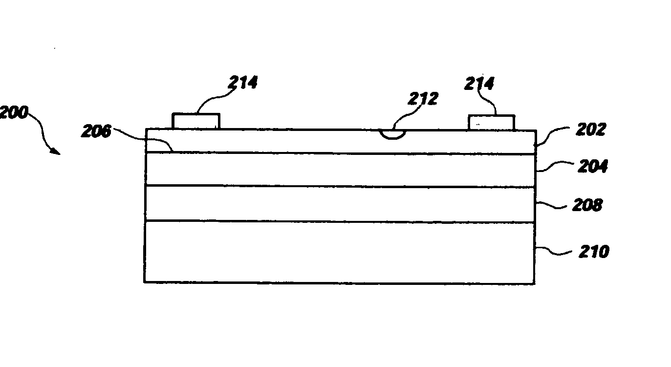
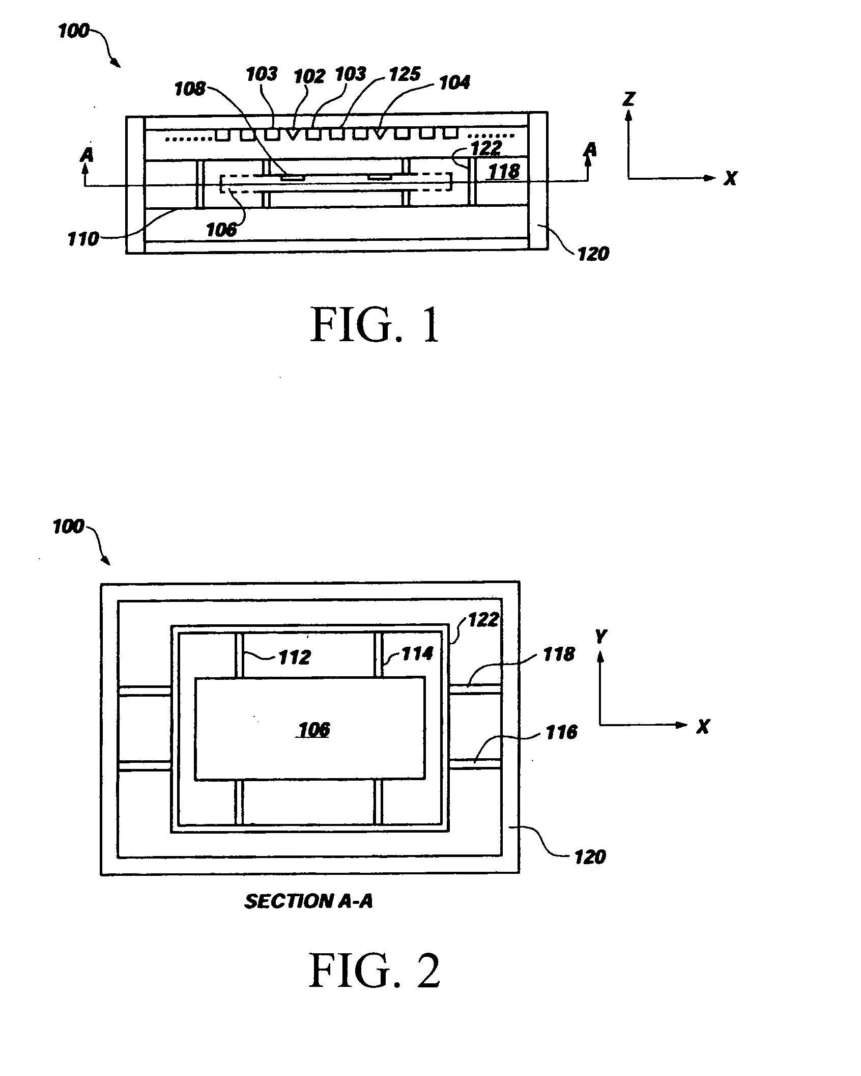
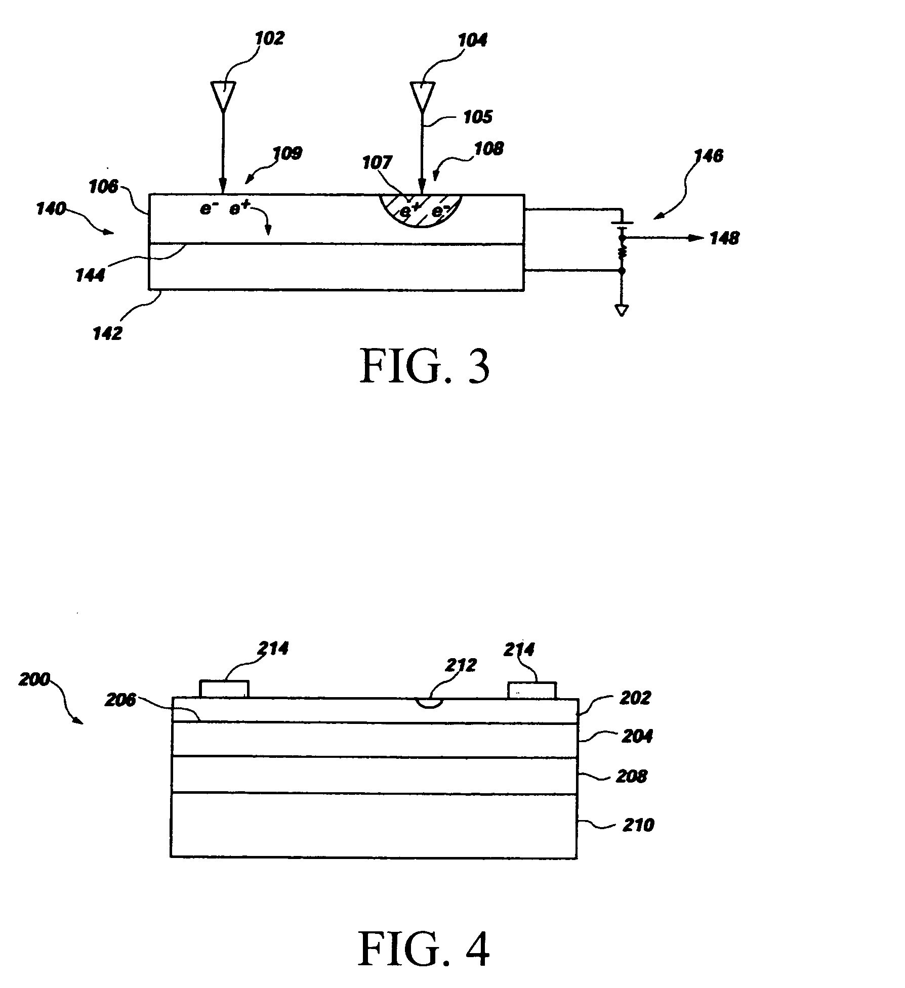
[0022]FIG. 1 shows an exemplary ultra-high density data storage system 100 having electron emitters 102 and 104 and a phase-change data storage medium 106. Electron emitter 102 and 104 are mounted above the storage medium 106, that has a number of storage areas, such as 108, that are impacted by electron beams from the emitters. Micromovers, based on micro-electromechanical systems (MEMS) technology, cause rela...


PUM


Abstract

An ultra-high density data storage device using phase-change diode memory cells, and having a plurality of emitters for directing beams of directed energy, a layer for forming multiple data storage cells and a layered diode structure for detecting a memory or data state of the storage cells, wherein the device comprises a phase-change data storage layer capable of changing states in response to the beams from the emitters, comprising a material containing copper, indium and selenium. A method of forming a diode structure for a phase-change data storage array, having multiple thin film layers adapted to form a plurality of data storage cell diodes, wherein the method comprises depositing a first diode layer of material on a substrate, and depositing a second diode layer of phase-change material on the first diode layer, the phase-change material containing copper, indium and selenium.

Description

FIELD OF THE INVENTION [0001] The present invention relates to ultra-high density data storage devices. More particularly, the present invention involves ultra-high density data storage devices having diode memory cells using materials containing copper, indium, and selenium, and methods of fabricating the diode memory cells. BACKGROUND OF THE INVENTION [0002] Electronic devices, such as palm computers, digital cameras and cellular telephones, are becoming more compact and miniature, even as they incorporate more sophisticated data processing and storage circuitry. Moreover, types of digital communication other than text are becoming much more common, such as video, audio and graphics, requiring massive amounts of data to convey the complex information inherent therein. These developments have created an enormous demand for new storage technologies that are capable of handling more complex data at a lower cost and in a much more compact package. Efforts are now underway to enable th...

Claims


Application Information

Patent Timeline
IPC IPC(8): G11B9/00G11B9/10G11B11/00G11B11/08H01L27/105H01L45/00
CPCB82Y10/00G11B9/10G11B9/14G11B11/08G11B9/1463G11B9/149G11B11/002G11B9/1409
Inventor ASHTON, GARY R.DAVIDSON, ROBERT J.
Owner HEWLETT PACKARD DEV CO LP
Learn More