Ultra-high density single-walled carbon nanotube horizontal array and its controllable preparation method

Inactive Publication Date: 2017-08-31
PEKING UNIV
View PDF2 Cites 1 Cited by
  • Summary
  • Abstract
  • Description
  • Claims
  • Application Information

AI Technical Summary

Benefits of technology

The patent describes a method for creating a high-density array of single-walled carbon nanotubes, which have been characterized using atomic force microscope (AFM) and scanning electron microscope (SEM) images. The results show that the density of the prepared nanotubes is up to 1,300 tubes per micrometer, which is the highest reported to date. The electrical performance test also shows that the on-current density and transconductance of the prepared nanotube array are the highest in the field effect transistor in the world at present. This demonstrates the high quality and density of the ultra-high density carbon nanotube array prepared using the present invention.

Problems solved by technology

However, with the development of the technology, more and more micro-transistors are integrated onto a single chip, the yield of good product in production and processing is reduced.
Silicon transistor is already close to atomic level and reaches to its physical limit, and it is very difficult to get breakthrough on the running speed and performance of the silicon transistor.

Method used


Image

  • Ultra-high density single-walled carbon nanotube horizontal array and its controllable preparation method
  • Ultra-high density single-walled carbon nanotube horizontal array and its controllable preparation method
  • Ultra-high density single-walled carbon nanotube horizontal array and its controllable preparation method

Examples


example 1

h of an Ultra-High Density Single-Walled Carbon Nanotube Horizontal Array

[0050]1) the pretreating of the single crystal growth substrate;

[0051]A-plane α alumina single crystal substrate is selected as the substrate for growing carbon nanotubes, and it is cut into a size of 4 mm×6 mm, wherein the side of 4 mm length is parallel to [0001] direction, and the side of 6 mm length is parallel to [1-100] direction. This substrate is pretreated as follows:

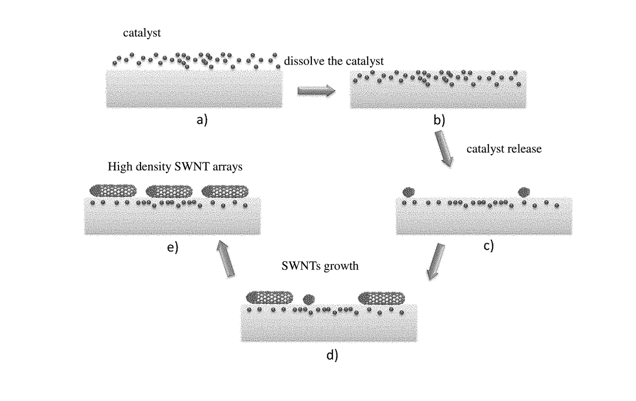
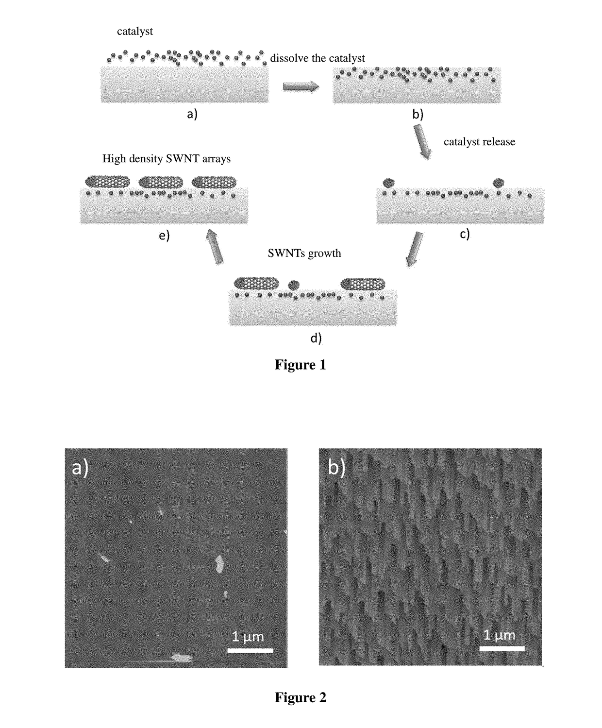
[0052]successively ultrasonic cleaning in secondary water, acetone, ethanol, and secondary water respectively for 10 min, and then blow-dried with high purity nitrogen, and its surface morphology is shown as FIG. 2a);

[0053]placing the cleaned substrate into a muffle furnace, and elevating the temperature from room temperature to 1100° C. within 2 h, then keeping 1100° C. of constant temperature for 8 h, then cooling to 300° C. within 10 h, and then naturally cooling to room temperature, so as to obtain a pretreated single crystal growth su...

example 2

h of an Ultra-High Density Single-Walled Carbon Nanotube Horizontal Array

[0064]step 1): which is same as the step 1 in example 1;

[0065]steps 2) and 3): after the Fe(OH)3 / EtOH solution used in example 1 is replaced with a (NH4)6Mo7O4 / EtOH solution of (NH4)6Mo7O4 with a concentration of 0.01 mmol / L, it is spin-coated on a-plane α alumina single crystal substrate according to step 3) in example 1, that is, the catalyst containing Mo is loaded on the surface of this a-plane α alumina single crystal substrate.

[0066]4) annealing

[0067]This substrate is placed into a muffle furnace to undergo an annealing at high temperature in the air, the temperature being elevated to 1000° C. from room temperature within 1.5 h, and kept constant at 1000° C. for 16 h, then cooled to 300° C. within 10 h, followed by naturally cooled to room temperature to complete the annealing step.

[0068]5) the oriented growth of single-walled carbon nanotubes using a chemical vapor deposition method:

[0069]the single crys...

example 3

nism Analysis of the Preparation Method of the Ultra-High Density Single-Walled Carbon Nanotube Horizontal Array

[0071]1) the analysis and validation of the incorporating mechanism in the preparation method of the ultra-high density single-walled carbon nanotube horizontal array;

[0072]XPS depth analysis is conducted on the annealed single crystal growth substrate obtained in step 4) of example 1, as shown in FIG. 5, Fe element is found underneath the surface of the alumina single crystal substrate, obviously, Fe catalyst can indeed get into the alumina single crystal substrate for storing by the above annealing method.

[0073]2) the analysis and validation of the release mechanism in the preparation method of the ultra-high density single-walled carbon nanotube horizontal array;

[0074]Annealing treatment is performed with hydrogen on the single crystal growth substrate obtained in step 4) of example 1 in a tube furnace, the flow gas of hydrogen being 100 sccm, and the treatment time (th...


PUM

PropertyMeasurementUnit
Temperatureaaaaaaaaaa

Abstract

The present invention discloses single-walled carbon nanotubes horizontal arrays with ultra-high density and the preparation method. The method comprises the following steps: loading a catalyst on a single crystal growth substrate; after annealing, introducing hydrogen into a chemical vapor deposition system to conduct a reduction reaction of the catalyst; and maintaining the introduction of the hydrogen to conduct the orientated growth of a single-walled carbon nanotube. The density of the ultra-high density single-walled carbon nanotube horizontal array obtained by this method exceeds 130 tubes / micrometer, and an electrical performance test is performed on the prepared ultra-high density single-walled carbon nanotube horizontal array shows a high on-current density of 380 μA / μm, and the transconductance of 102.5 μS / μm.

Description

TECHNICAL FIELD[0001]The present invention belongs to semiconductor field, and relates to an ultra-high density single-walled carbon nanotube horizontal array and its controllable preparation method.BACKGROUND[0002]Single-walled carbon nanotubes (SWNTs) have attracted great concerns of nanotechnology researchers since they were found in 1993 due to their special structures and excellent properties. Owing to their high toughness, strong electrical conductivity, excellent field emission property, and metallic and semiconducting properties, SWNTs, referred to as “super fiber”, are considered as one of the host materials in nano-electronic devices at post-Moore era. At present, an extensive research is being conducted on potential applications of SWNTs, including quantum wire, electronic device, composite material, electroluminescence, photoluminescence, chemical sensor, nanoparticle carrier and so on.[0003]As for chip industry, traditional transistors are made up of silicon. However, w...

Claims


Application Information

Patent Timeline
IPC IPC(8): H01L51/00C30B25/18C30B29/02C30B29/20C30B31/04H01L51/05C23C16/26C23C16/02C23C16/455B05D1/00B05D3/04B05D3/00C01B31/02
CPCC01B31/0233Y10S977/938H01L51/0048H01L51/0566H01L51/0541C30B25/186C30B29/02C30B29/20C30B31/04C23C16/26C23C16/0272C23C16/45512B05D1/005B05D3/0453B05D3/0406B05D3/007B05D1/60C01B2202/02B82Y40/00B82Y30/00Y10S977/75Y10S977/843H01L51/0002C01B2202/08C01B2202/22C01B32/162B82Y10/00C30B29/60H10K85/221H10K10/484H10K10/464H10K10/488H10K71/10
Inventor ZHANG, JINHU, YUEKANG, LIXINGZHAO, QIUCHENZHANG, SHUCHEN
Owner PEKING UNIV
Why Eureka
Try Eureka