Method for the manufacture of an active matrix, corresponding electro-optical display devices and mask

a technology of electro-optical display and active matrix, which is applied in the direction of photo-taking processes, instruments, photomechanical apparatuses, etc., can solve the problems of affecting the reproduction of images or designs, and affecting the accuracy of image reproduction

Active Publication Date: 2005-04-07
INTERDIGITAL CE PATENT HLDG
View PDF7 Cites 7 Cited by
  • Summary
  • Abstract
  • Description
  • Claims
  • Application Information

AI Technical Summary

Problems solved by technology

These defects are especially edge effects, magnification, optical aberration, rotation and x-axis or y-axis misalignment of the mask.
They cause imprecision in the reproduction of the image or design at the boundary or junction between two successive exposure fields.
This is the defect known as the “stepper pattern” defect which acts on the electro-optical qualities of the display device.
These couplings are sensitive to the defects of the designs of the gates, the semiconductor layers, columns and drains of the TFTs and pixel electrodes.
In practice, this break implies difficulty in accurately restoring the gray levels.
There is therefore a deterioration in visual quality.
In this peripheral zone of the mask, the design to be made is incomplete or fuzzy.

Method used


Image

  • Method for the manufacture of an active matrix, corresponding electro-optical display devices and mask
  • Method for the manufacture of an active matrix, corresponding electro-optical display devices and mask
  • Method for the manufacture of an active matrix, corresponding electro-optical display devices and mask

Examples


Embodiment Construction

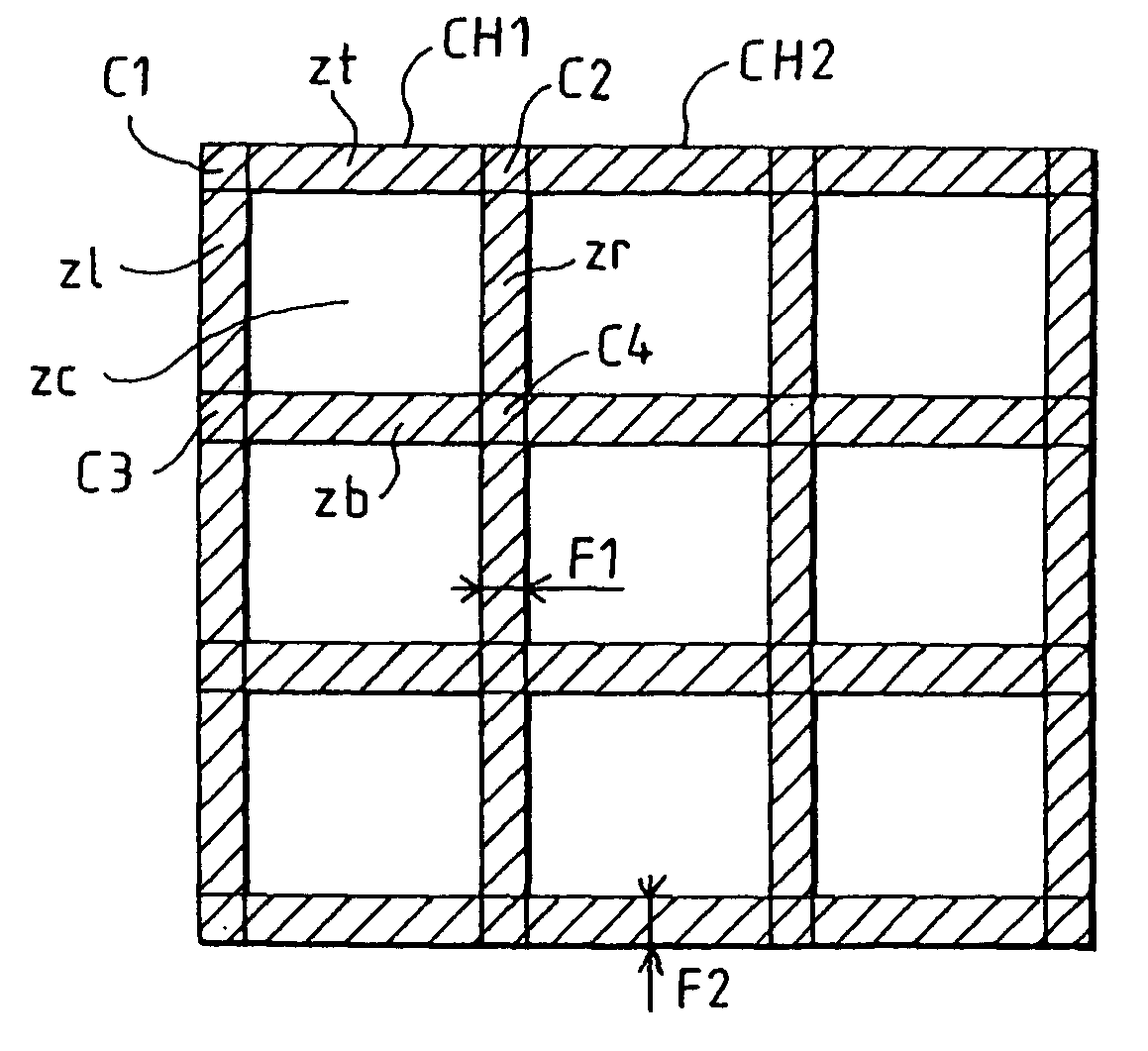
[0043] The principle of exposure according to the invention is illustrated in FIG. 4, which shows an overlap zone ZR with a width F overlapping two exposure fields INS1 and INS2. These insulation fields have been obtained from a mask, to reproduce an identical pattern m at each dot of the active matrix.

[0044] Each exposure field has a zone in which all the patterns m are made and a peripheral zone in which only certain patterns are made. A first exposure of the mask is made, giving a first exposure field INS1. A second exposure of the same mask is made, in placing the mask in such a way that the peripheral zone of the mask gets superimposed on the peripheral zone of the previously exposed field. The figure shows the right-hand lateral boundary LI1 of the exposure. The left-hand lateral peripheral part of the mask is superimposed on the right-hand lateral peripheral part of the first field INS1 to make the second exposure field INS2. The overlap zone ZR on the active matrix is thus ...


PUM

PropertyMeasurementUnit
densityaaaaaaaaaa
widthaaaaaaaaaa
polarityaaaaaaaaaa

Abstract

In a method for the manufacture of an active matrix for an electro-optical display device, the active zone exposure fields CH1, CH2 are obtained by the transfer of an active zone mask in such a way that there is a non-null overlap zone zl, zr, zt, zb between two successive exposure fields. The active zone mask is exposed a first time. This mask is positioned for the next exposure so as to overlap the first exposed field on a certain width F1, F2. In the overlap zones, an exposure of the mask provides only a part of the patterns.

Description

BACKGROUND OF THE INVENTION [0001] 1. Field of the Invention [0002] The present invention relates to a method for the manufacture of active matrices for electro-optical display devices. It can be applied especially to the manufacture of high-density flat screens. It can be applied more generally to matrix display devices used in direct viewing or in projection. [0003] To put it in simple terms, an active matrix display device comprises cells arranged in a crossed array of rows and columns, each cell comprising a pixel associated with an electronic switch. This switch is formed by an active element, which may be a transistor or a diode, that is electrically connected to a column of the array and connects the pixel to a row of the array. These cells are all identical. They are obtained from the same pattern at each level of manufacture. These cells form the active zone of the matrix circuit. Control and addressing circuits for the rows and columns of the matrix are positioned at the p...

Claims


Application Information

Patent Timeline
Patent Type & Authority Applications(United States)
IPC IPC(8): G02F1/1362G03F1/00G03F7/00G03F7/20H01L21/77H01L21/84H01L27/12
CPCG02F2001/13625G03F1/144G03F7/0007H01L27/1288G03F7/70475H01L27/1214G03F7/70433G03F1/00G02F1/13625
Inventor SALUEL, DIDIERTERRIEN, JEAN-CHARLESLEBRUN, HUGUES
Owner INTERDIGITAL CE PATENT HLDG
Why Eureka
Try Eureka